EU Establishes ELENA Network for Study of Nanotechnology Processes, Including FEBID Additive Manufacturing Technique

 Nanotechnology proves that bigger isn’t always better. The technology is engineering, science, and technology at the nanoscale, which operates at one billionth of a meter. Think of it this way: a single sheet of newspaper is about 100,000 nanometers thick. Nanotechnology allows objects that are only a few hundred nanometers “to be produced in any required shape.” There all sorts of applications for these tiny objects: microprocessors and electrical circuits in computers, medicine and biotechnology, and many others. Researchers at Virginia Tech used 3D printing to scale nanotechnology up, to see if the special mechanical properties were still there, and if so, if they could be controlled. The European Union (EU) recently established the Marie Curie Training Network ELENA (low energy electron-driven chemistry for the advantage of emerging nanofabrication methods) as a way to encourage the development of new manufacturing processes.
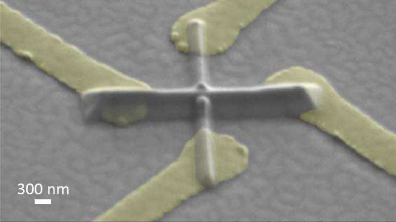
A magnetic sensor additively written with a focused electron beam and Co2(CO)8 molecules, located between four previously-structured gold electrodes. The sensor can be given any required shape by moving the substrate or adjusting the dwell time of the electron beam. [Credit: Swiss Federal Laboratories for Materials Science and Technology]
Empa had been previously involved in ELENA’s predecessor, the COST-Action Network CELINA (chemistry for electron-induced nanofabrication), which investigated how suitable low volatility materials were for “directly writing with focused electron beams” using an in-house developed gas injection system, with a scanning electron microscope.
![]() The EU will make about €4 million in funding available for ELENA over the next four years, so the network can focus on two cutting-edge nanotechnology processes: Focused Electron Beam Induced Deposition (FEBID) and Extreme Ultraviolet Lithography (EUVL). The first of these two techniques utilizes a form of additive manufacturing, and is utilized by Oak Ridge National Laboratory, which recently improved on the process. TU Wien researchers even got the FEBID method to yield pure gold, after a co-injection of an oxidative enhancer.
The EU will make about €4 million in funding available for ELENA over the next four years, so the network can focus on two cutting-edge nanotechnology processes: Focused Electron Beam Induced Deposition (FEBID) and Extreme Ultraviolet Lithography (EUVL). The first of these two techniques utilizes a form of additive manufacturing, and is utilized by Oak Ridge National Laboratory, which recently improved on the process. TU Wien researchers even got the FEBID method to yield pure gold, after a co-injection of an oxidative enhancer.
The FEBID technique uses an extremely finely focused electron beam from a scanning microscope to “write” 3D structures on a surface’s shape, like the silicon wafers that are used to make tiny computer chips. The structures are actually created with a type of additive manufacturing: absorbing molecules are “continuously supplied to the surface in question,” and the electron beam then breaks these up. Then, certain parts of the molecule are “locally deposited onto the substrate.” The FEBID process needs “molecules containing the necessary component parts,” which are later freed by the same focused electron beam in order to make the “required material composition on the substrate.”
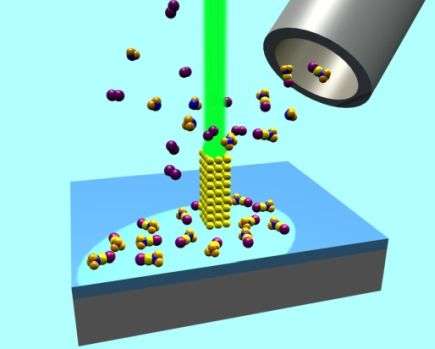
FEBID: within a scanning electron microscope molecules supplied continuously to a point on the surface are locally decomposed by a focused electron beam. This creates an “Additive Manufacturing” platform with a lateral resolution of less than 10 nm. [Credit: Swiss Federal Laboratories for Materials Science and Technology]
The second nanotechnology process that the ELENA partners will study, EUVL, also “imprints extremely fine structures on surfaces,” although only in two dimensions, and not three, like FEBID. EUVL also requires specially adapted materials, thin films called photoresists, in order to function correctly. When EUV light irradiates the photoresists correctly, they “efficiently and precisely create the required structures.”
The 15 doctoral students working on the ELENA project are specifically focused on the search for new molecules that can be used for “additive writing” on pure metals with the FEBID process, and new photoresists for the EUVL process. Discuss in the ELENA forum at 3DPB.com.
[Source: Empa]Subscribe to Our Email Newsletter
Stay up-to-date on all the latest news from the 3D printing industry and receive information and offers from third party vendors.
Print Services
Upload your 3D Models and get them printed quickly and efficiently.


You May Also Like
Thrōn made Launches Kickstarter Campaign for 3D Printed Furniture Made with Recycled Material
This month, a small U.S. startup called Thrōn made launched a crowdfunding campaign on Kickstarter for its collection of 3D printed sculptural furniture, with an emphasis on sustainable, eco-friendly solutions....
FibreSeeker 3: The World’s First Continuous Fibre 3D Printer for the Consumer Launches on Kickstarter
For decades, FDM 3D printing has been the go-to technology for makers, engineers, and educators looking to quickly prototype ideas. But while the speed and accessibility of fused deposition modeling...
3D Printing News Briefs, September 6, 2025: SBIR Awards, Regenerative Medicine, & More
In this weekend’s 3D Printing News Briefs, we’ll start with some exciting funding news, as NIST has awarded over nearly $2 million to small businesses working to advance AI, additive...
From Energy to Defense: Strengthening Supply Chains Through Dual-Use Additive Manufacturing
Dual-use technologies serve more than one sector, often bridging the gap between commercial and defense applications. Additive manufacturing (AM), once seen primarily as a prototyping tool, is now maturing into...