TU Wien: Researchers 3D Print Gold Using Basic Compounds & Electron Beams


 The thought of winning the lottery, finding the pot of gold at the end of the rainbow, hidden treasure, or the goose that lays the golden egg is always enticing. While most of us see these ideas as grand hopes that are fun to think about but will never happen, there are sometimes the lucky few we see in a lifetime who happen upon something so incredible that it quite simply changes everything. As to what changes, and how important it is to you, may be a matter of perspective, but when it comes to science, often we are just seeing the precursor to something that is indeed revolutionary and will spark off countless other spectacular innovations.
The idea of just being able to re-create an item like a precious metal is also something many dream about, but the path to such a thing is one that—even in just experimenting—requires great education and previous scientific experience, enormous effort and dedication, and many hours tucked away working in a lab with an extensive setup. With all of those human ingredients in place, now it would appear that researchers from TU Wien have indeed made one of those breakthroughs, cracking the code for making pure gold in the form of very valuable nanostructures.
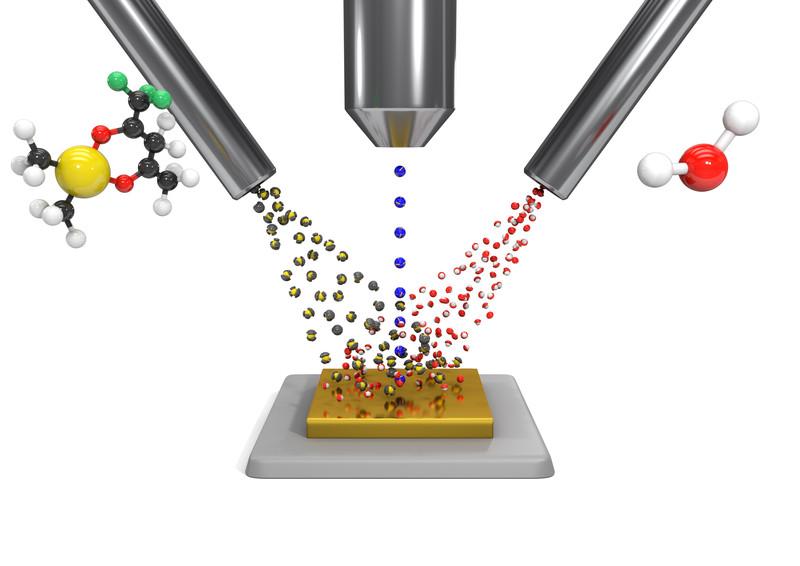 Creating a unique direct-write lithography method, these researchers can actually turn an ‘auriferous organic compound’ directly into gold. With their findings outlined in ‘Highly conductive and pure gold nanostructures grown by electron beam induced deposition,’ authored by Mostafa M. Shawrav, Philipp Taus, Heinz D. Wanzenboeck, M. Schinnerl, M. Stöger-Pollach, S. Schwarz, A. Steiger-Thirsfeld and Emmerich Bertagnolli, the researchers share that they are able to create any number of shapes, albeit very very tiny, with their new technique, which uses a gold content of 91 atomic percent—accomplished as they used water to enhance the printing process.
“Co-injection of an oxidative enhancer enabled Focused Electron Beam Induced Deposition (FEBID)—a maskless, resistless deposition method for three dimensional (3D) nanostructures—to directly yield pure gold in a single process step, without post-deposition purification,” state the researchers in their paper.
“This is the highest conductivity achieved so far from FEBID and it opens the possibility of applications in nanoelectronics, such as direct-write contacts to nanomaterials,” said the researchers. “The increased gold deposition yield and the ultralow carbon level will facilitate future applications such as the fabrication of 3D nanostructures in nanoplasmonics and biomolecule immobilization.”
This work is unique in that it offers a highly specialized process for creating pure and conductive gold structures, and without any later purification being required, due to the introduction of the water vapor with the ‘organometallic precursor’ simultaneously.
“Gold is not only a noble metal of exceptional beauty, but also a highly desired material for functional nanostructures,” says Professor Heinz Wanzenböck from TU Wien.

Up until now, the obstacle in producing pure gold nanostructures has been that of making them not just on non-planar surfaces, but also in 3D. In quite a research milestone, the team from TU seems to have solved this, and forged beyond with the use of the electron beam. Due to the extreme precision allowed, the beam breaks down the compounds beneath it, with the result being gold that is not only 3D, but solid; in fact, it is, according to TIU, only a factor 4 away from the bulk resistivity of purest gold. Here, a great deal of experimentation by experts has finally brought something amazing to fruition, with the printing of real gold—and the potential for a whole new level of nanoelectronics to explode in the future.
“The whole community has been working hard for the last 10 years to directly deposit pure gold nanostructures,” says Wanzenböck. “It’s a bit like discovering the legendary philosopher’s stone that turns common, ignoble material into gold.”
Discuss in the 3D Printed Gold forum at 3DPB.com.
[Source/Images: Tu Wien]Subscribe to Our Email Newsletter
Stay up-to-date on all the latest news from the 3D printing industry and receive information and offers from third party vendors.
Print Services
Upload your 3D Models and get them printed quickly and efficiently.


You May Also Like
Phillips Corporation Rebrands Additive Hybrid Division, Now Called Phillips Advanced Manufacturing
Phillips Corporation announced that it will rebrand its Additive Hybrid division to become Phillips Advanced Manufacturing. The focus will now be on advanced manufacturing in the broadest sense. Brian Kristaponis...
Arridex Opens Additive Manufacturing Omnifactory in Lagos for MRO & Spare Parts
Arridex, formerly known as the RusselSmith Group, has been building additive manufacturing competence and capacity in Africa for years. Previously, the company got approval to use a Roboze 3D printed...
DREAMing in Dayton: DREAM Symposium Covers AM, AI, Supply Chain, & More
This month, I attended a manufacturing industry event, like I often do. But instead of getting on a plane to New York City, or driving four hours to Youngstown, I...
ORNL Origami Creates Large Foldable Structures
Oak Ridge National Laboratory (ORNL) is using a hybrid 3D printing method to make foldable panels. At the Department of Energy’s (DOE) Manufacturing Demonstration Facility (MDF) at ORNL, researchers turned...