
ORNL Researchers Improve 3D Printing at the Nanoscale with Simulation Guided Process


 You may have noticed that 3D printing seems to be getting bigger and bigger by many accounts, from 3D printed cars to buildings, and even entire villages. As the skill and knowledge are increasing with this new technology around the world, so are the equipment and the innovations themselves. For many researchers involved in reaping the rewards of 3D printing, however, they operate on the opposite of the ‘bigger is better’ motto, working with the tiniest of structures.
While many of us can barely even comprehend what happens in the realm of the nano, for researchers like the team at Oak Ridge National Laboratory in Tennessee, that’s not just where they are comfortable—the nanoscale is where they get excited. That doesn’t mean their work at ORNL is easy, however. And in their latest project, they were working to streamline the process of designing and 3D printing structures you can’t even see.
A nano denotes something very small. As small as 1/1000 of a hair, in fact. And if you had to work with something on that scale, as well as attempting to 3D print it, you’d probably be devoting some time to finding better ways to do so as well. Consider your first attempts at 3D printing, designing a model.
“Imagine shrinking it smaller than a drop of water, smaller even than a human hair, until it is dwarfed by a common bacterium,” offers an ORNL press release.
For nanoscale fabrication, the researchers use focused electron beam induced deposition (FEBID). This is definitely not the 3D printing you’ve been trying from the desktop, but it does make sense if you consider what is really a simple process—just for much smaller things—with the beam from the scanning microscope creating a solid deposit upon condensing gaseous precursor molecules. While that certainly sounds impressive and actually is somewhat easy to visualize, it’s also not all that surprising to find that the method was considered difficult, error-prone and impractical unless just 3D printing structures over several nanometers. As a solution, the team at ORNL, in collaboration with the University of Tennessee and the Graz University of Technology, created a new process.
As team leader Jason Fowlkes of the ORNL Center for Nanophase Materials Sciences, a DOE Office of Science User Facility, explained, the secret for improvement was in combining both design and construction into one act, streamlining, and further allowing the team to make 3D printed nanostructures that are complex.
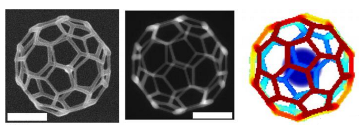
A 32-face 3-D truncated icosahedron mesh tested the simulation’s ability to make complex geometries. The SEM image of the final experimental product (left) was highly consistent with the structure predicted by the virtual SEM image (center) and the simulated design model (right). [Image: ORNL]
Here, the team discusses how the old approach in 3D printing wasn’t quite right for the context of their projects:
“While the fabrication of simple architectures such as vertical or curving nanowires has been achieved by simple trial and error, processing complex 3D structures is not tractable with this approach. In part, this is due to the dynamic interplay between electron–solid interactions and the transient spatial distribution of absorbed precursor molecules on the solid surface.”
In applying 3D lattice structures at the micro/nanoscale, they achieved very good results—so good in fact, that in the paper, they discuss the amount of considerable attention received due to the ‘superior mechanical and optical properties’ they have achieved.
Because the team has found such an accurate ability to design custom nanostructures, Harald Plank, from Graz, and one of the co-authors of the paper, sees this study as having opened up ‘a host of novel applications in 3D plasmonics, free-standing nano-sensors and nano-mechanical elements on the lower nanoscale which are almost impossible to fabricate by other techniques.’
With 3D simulation in guiding the beam, the researchers are able to make both their lattices and their meshes between 10 nanometers and one micron. The 3D printing method happens as electron scattering paths are tracked, along with the release of the secondary electrons, allowing for the prediction of the deposition pattern, and the consequent visualization of the structure.

Jason Fowlkes
What makes this new process special is the combination of both the simulation and the experiments, says Fowlkes. The construction is guided by the simulation, and the completed experiments allow for feedback on both the accuracy and the strength of the simulation itself.
Inconsistencies caused by secondary electron activity can be filtered out easily as well, caught as designs are being fed into simulation and drafting.
“In its simplest form, once we know the emission profile of those secondary electrons we don’t want, we can design around them,” Fowlkes said.
And although it may be slower than other methods used to make structures on the nanoscale, Fowlkes stresses that the FEBID process is the only way to make the 3D printed high fidelity nanostructures they have been producing. Otherwise, they revert back to the trial and error method with manual adjustments required to get the desired outcome.
Now they will be able to focus on further refinements such as clearing the 3D printed structures of carbon contamination, through an in situ purification process. This is performed through using water, oxygen, and a laser, removing the carbon. According to ORNL, during the simulation, both the stresses of the removal process and the transformation to be found in the final product can be anticipated.
“We can design structures in a way where the actual writing pattern might look distorted, but that’s taking into account the fact that it’s going to retract and contract during purification and then it will look like the proper structure,” Fowlkes said.
This research was supported by the Center for Nanophase Material Sciences, a DOE Office of Science User Facility. Discuss further over in the ORNL Metal 3D Printing forum at 3DPB.com.
[Source: ORNL]Subscribe to Our Email Newsletter
Stay up-to-date on all the latest news from the 3D printing industry and receive information and offers from third party vendors.
Print Services
Upload your 3D Models and get them printed quickly and efficiently.


You May Also Like
Divergent Declares that German 3D Printers are Superior, And Plans Massive LPBF Expansion
Divergent has announced a new version of its Laser Powder Bed Fusion (LPBF) printer and a new site. The company aims to do nothing short of “further accelerating its mission...
Incodema3D Buys 14 Metal EOS Systems, Now One of the World’s Largest Metal 3D Printer Operators
Recently, a majority stake of 3D printing service bureau Incodema3D was purchased by AFM Capital. Under new ownership, the Freeville, New York company is now using its cash-rich parent for...
CEO Yoav Zeif on Why Stratasys’ Markforged Acquisition Is Really a Bet on Industrialization
When Stratasys announced plans to acquire Markforged, the immediate focus was on the deal. Markforged is one of the most recognizable names in additive manufacturing (AM), known for its continuous...
3D Printing & the Autonomous Era: Defense Tech’s Latest Mutation
When we last checked in on the broad defense tech landscape and the role of the additive manufacturing (AM) industry in that environment, it became clear that the connecting thread...