AI & Camera Monitoring of 3D Printed Electronics for Quality Assurance


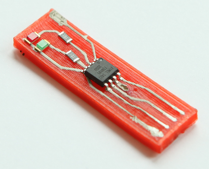
Since 2009, Neotech AMT GmbH, based in Nuremburg, Germany, has been working to develop technologies for 3D printing electronics, and several years ago combined Aerosol Jet Printing (AJP) with its own five-axis print motion platform to enable direct write printing of electronics, such as 3D molded interconnect devices, for a variety of markets, including automotive, medical, mobile communications, and wearables.
Now, the company is partnering with researchers from the University of Hamburg to make electronics 3D printing more reliable, and scalable for industrial applications, by creating a quality assurance (QA) system driven by a camera and artificial intelligence (AI).
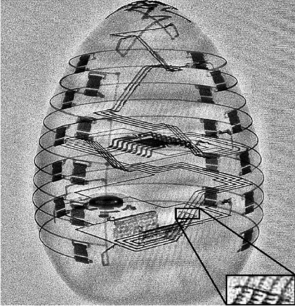
X-Ray image of 3D printed device (Image courtesy of FAPS)
“This project is an important step towards closed loop control for hybrid manufacturing processes,” explained Dr. Florens Wasserfall from the University of Hamburg. “Variations in quality and accuracy have been a major limitation ever since the invention of additive technologies. Active process monitoring is a core aspect to enable reliable and scalable manufacturing of highly integrated, smart products.”
Together with the university’s TAMS Group (Technical Aspects of Multimodal Systems), which is led by Prof. Dr. Jianwei Zhang, Neotech is developing an AI- and camera-based monitoring system to be used for 3D printing objects with integrated electronics. The work is called Project KamEl, and will continue for quite some time, with a projected end date in September 2022. The Central Innovation Program for SMEs (ZIM) from Germany’s Federal Federal Ministry for Economic Affairs and Energy (BMWi) is providing the funding for this 3D printed electronics monitoring system project.
Project KamEl (Image courtesy of University of Hamburg)
“Automated Quality Assurance (QA) will be developed with which the manufacturing processes can be monitored online in the 5-axis manufacturing cell,” the Project KamEl site states.
So, here’s how it works: the 3D printing process will be recorded and classified, and, dependent on what kind of processing errors show up, the platform will automatically correct them. Specifically, the printed electrical structures will be recorded in 3D space by the vision system, and the platform will assemble the images together, making sure to compensate for depth of field elements and potential distortion.
AI-enabled image processing is used to recognize the prints in order to check for defects, such as short circuits, line breaks, and geometrical errors in thickness and width. If the platform determines there is a defect in the print, the AI system will choose the correct option, out of three possibilities, that should fix it:
- automated correction by the system
- correction with input from the operator
- part rejection, which stops the print
This correction thus creates a closed-loop system of the conductive track 3D printing process.
(Image courtesy of University of Hamburg)
“This exciting development opens the way for guaranteed QA and traceability in “Fully Additive” 3D Printed Electronics whist also increasing product yields,” said Dr. Martin Hedges, the Managing Director of Neotech AMT. “The risk of defects only being discovered after lengthy manufacturing processes is mitigated and autocorrection will bring yield losses to an absolute minimum.”
Additionally, the data that this closed loop system creates will be archived for documentation, so the KamEl team can support certifications in important applications.
(Source: Neotech AMT GmbH)
Subscribe to Our Email Newsletter
Stay up-to-date on all the latest news from the 3D printing industry and receive information and offers from third party vendors.
Print Services
Upload your 3D Models and get them printed quickly and efficiently.


You May Also Like
3D Printing News Briefs, July 9, 2026: RIMPAC 2026, Software, Housing, & More
In today’s 3D Printing News Briefs, Massivit continues its focus on aerospace and defense manufacturing, and Meltio is collaborating with Phillips Corporation for RIMPAC 2026. Moving on to software, AMIS...
3DPOD 304: Precast Concrete AM with Greg Kerkstra, Mangrove
Greg Kerkstra is part of a family business that leads in the precast concrete industry. They’ve now turned to Progress Group’s large-format binder-jet concrete technology, which we covered here in...
3D Printing News Briefs, June 10, 2026: Grand Opening, Photoresins, Footwear, & More
We’re starting with some exciting news in today’s 3D Printing News Briefs: Stratasys just celebrated the opening of its new North American headquarters in Minnesota. Moving on, Nanoscribe is scaling...
Wells Fargo Backs ICON in Landmark Milestone for 3D Printed Housing
Qualification is an indispensable step on the path to legitimization for any new technology, but it’s still just one step: markets tend to remain unswayed without a co-sign from an...