Electronics 3D Printing Part Three: Inkjet 3D Printing


In our previous articles in this series, we discussed the history leading up to the development of electronics 3D printing, as well as one of the two dominant methods for printing electronics, direct writing. The other leading method for 3D printing electronics is inkjetting.
Inkjetting processes deposit photopolymers similar to a printhead found in 2D printers before curing them using ultraviolet light. The most notable company working with this process is NanoDimension, an Israeli company that has developed the DragonFly series of PCB 3D printers.
The DragonFly series jets conductive inks alongside a photocurable, dielectric ink. The process by printing bottom solder masks and pads, then printing and sintering conductive layers and printing and curing the dielectric layers, and then ending with the top solder masks and pads. The dielectric ink is cured with an LED lamp, while the conductive ink is sintered by an internal energy source.
Auxiliary electronics, including transistors and resistors, can then be added to prototype PCB designs, including multilayer PCBs. The company has demonstrated a number of applications, including embedded electronics, electromagnets, molded interconnect devices, antennas and sensors.
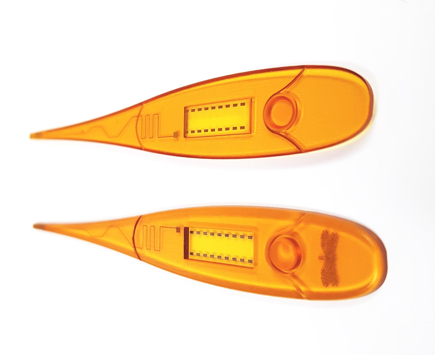
A 3D printed thermometer made using Nano Dimension technology. Image courtesy of Nano Dimension.
Like NanoDimension, ChemCubed inkjets dielectric photopolymer alongside conductive silver ink. The company’s flagship product is the ElectroJet, an LED flatbed 3D printer designed through a collaboration Direct Color Systems. Because Direct Color Systems offers UV printing machines—for Braille and textured signage, phone cases, acrylic awards and other applications— with build areas up to 600mm x 1,200mm in size, it’s possible that ChemCubed could scale up the size of its system to even enable batch additive production of PCBs.
A Boston startup with exciting potential is Inkbit, which is commercializing technology developed at MIT that combines inkjet technology with machine vision and learning to 3D print multi-component objects. The vision system scans each layer with micrometer resolution as the ink is deposited, registering any discrepancies between the print and the CAD geometry and compensating. This means that the internal roller required for evening layers in traditional inkjet systems, is unnecessary, allowing for the use of materials that would not jam these conventional types of systems. Meanwhile, the machine learning software behind Inkbit’s process is able to learn from errors that occur within prints and improve over time.
The machine vision system makes it possible to also incorporate additional parts into printed objects. To do this, the printer is paused and these items, such as metal reinforcement or electronics, can be manually inserted before the print begins and material is printed around them. At MIT’s Computer Science and Artificial Intelligence Laboratory, where the technology was developed, researchers demonstrated the ability to 3D print complex lenses, micro lens arrays, fiber-optic bundles, complex meta materials, an object with a built-in razor blade, lenses on top of LEDs, and even a plastic smartphone case around an existing smartphone. While the incorporation of these elements is currently performed manually, the company is hoping that, in the future, the Inkbit system can be brought into a production line where pick and place machines can add these components automatically.
Inkbit’s technology demonstrates the potential future of electronics 3D printing, having already tackled the ability to fabricate complete, functional objects with a single build process, though there is are a number of hurdles to overcome, not the least of which is automation. In our next post in the series, we will look at the myriad research endeavors currently being pursued to expand the capabilities of present electronics 3D printing technology.
Subscribe to Our Email Newsletter
Stay up-to-date on all the latest news from the 3D printing industry and receive information and offers from third party vendors.
Print Services
Upload your 3D Models and get them printed quickly and efficiently.


You May Also Like
3D Printing News Briefs, July 9, 2026: RIMPAC 2026, Software, Housing, & More
In today’s 3D Printing News Briefs, Massivit continues its focus on aerospace and defense manufacturing, and Meltio is collaborating with Phillips Corporation for RIMPAC 2026. Moving on to software, AMIS...
3DPOD 304: Precast Concrete AM with Greg Kerkstra, Mangrove
Greg Kerkstra is part of a family business that leads in the precast concrete industry. They’ve now turned to Progress Group’s large-format binder-jet concrete technology, which we covered here in...
3D Printing News Briefs, June 10, 2026: Grand Opening, Photoresins, Footwear, & More
We’re starting with some exciting news in today’s 3D Printing News Briefs: Stratasys just celebrated the opening of its new North American headquarters in Minnesota. Moving on, Nanoscribe is scaling...
Wells Fargo Backs ICON in Landmark Milestone for 3D Printed Housing
Qualification is an indispensable step on the path to legitimization for any new technology, but it’s still just one step: markets tend to remain unswayed without a co-sign from an...