
Electronics 3D Printing, Part One: History of Electronics 3D Printing


Perhaps the holiest of holy grails for the additive manufacturing (AM) industry is the fabrication of complete, functional goods within a single print operation. Rather than produce individual parts that must be assembled to form a final product, researchers and a handful of companies are pursuing this lofty goal, often focusing on electronics printing specifically as the biggest task to accomplish on the route to achieving that goal. Here we look at electronics 3D printing, how it began, the companies and researcher labs involved, its current state and where it is headed.
Printed electronics are already a mainstay of our technological world, with processes such as screen printing, flexography, gravure, offset lithography and inkjet used to produce a wide array of electronic components that are nearly ubiquitous. German inventor Albert Hanson is often attributed as conceiving of the idea, patenting “Printed Wires” in 1903 and proposing the idea of printed circuit boards formed by patterning copper foil via cutting or stamping.
The first printed circuits were developed by Austrian Paul Eisler in 1936 and consisted of drawn elements glued to dielectric paraffined paper. This process served the basis for mass production of printed circuit boards (PCBs) for radios and anti-aircraft shells by U.S. and British forces during World War II before commercialization began in 1948. To produce the circuits for these anti-aircraft proximity fuzes, the Centralab Division of Globe Union screenprinted metallic paint as conductor material and carbon resistor material onto ceramic plates, with ceramic disc capacitors and subminiature vacuum tubes then soldered in place.
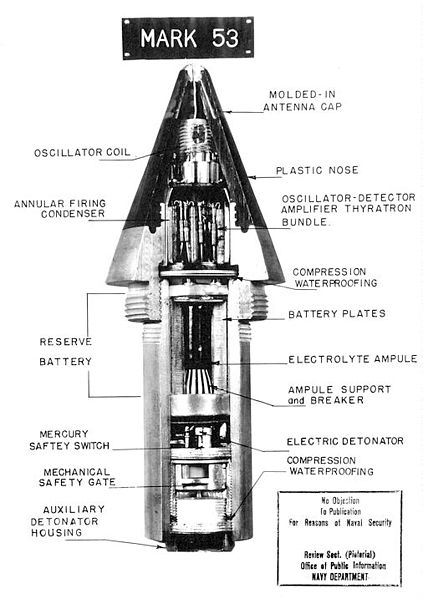
An MK53 fuze for anti-aircraft shells. Image courtesy of Wikipedia.
Additional developments that occurred to further automate the circuit printing process included the shift from through-hole construction, in which leads were inserted through chip holes and soldered to copper traces, to Auto-Sembly, wherein leads were dipsoldered onto copper foil. The invention of Auto-Sembly, combined with board lamination and etching, laid the foundation for existing PCB manufacturing. As through-hole parts have been replaced with small surface mounted components, boards have shrunken in size and, eventually, multilayer boards and high-density interconnect PCBs were developed.
IDTechEx anticipates the printed electronics market to reach $330 billion by 2027. Already numerous methods for printing electronics have become quite advanced, with MIT using inkjet printing to create a flexible solar cell using standard paper and Rice University creating organic solar cells that can be painted onto 3D surfaces. RFID chips are now embedded in most newer smartphone models, with the RFID manufacturing process relying heavily on the electronics printing steps outlined in the video below:
For mass producing PCBs, photo plotters created master circuit patterns that were drawn on clear mylar or glass, which was then transferred onto a copper coated laminate and layered with positive photoresist material. Exposed to light, any piece of photosresist that wasn’t masked became soluble and could be washed away. Exposed copper was then etched away to leave only the desired circuit pattern. The board could then be mounted with resistors, capacitors and integrated circuits.
This process is limited by the need to maintain a master artwork or create a new master artwork just to make modifications to an existing pattern. Photo plotting, as well as inkjetting and screen printing, involve the printing of circuits onto flat surfaces, thus limiting their implementation.
3D printing has sought to introduce its strength in manufacturing batches of specialized parts to the world of electronics manufacturing. There are various ways that this has been accomplished, including the spray deposition of electronic circuits onto 3D substrates, as well as the inkjetting of circuits into thermoset and thermoplastic parts.
In the 1990s, the Defense Advanced Research Program Agency (DARPA) pursued an electronics printing project Mesoscale Integrated Conformal Electronics, in which electronics could be made directly from CAD models using a wide variety of materials in a conformal manner on virtually any substrate. The result was Aerosol Jet technology from Optomec, which is capable of spraying conductive inks onto 3D substrates. We will discuss Aerosol Jet in our next article, but it’s important to fit it in here as what is we believe to be the first commercial electronics 3D printing technology, commercialized in 2003.
Another early pioneer in the space was Hod Lipson, whose labs at Cornell and Columbia have sought to manufacture whole functional devices within a single build process starting as early as 2004. This video from 2013 showcases a loudspeaker that was printed using the open source Fab@Home 3D printer developed in Lipson’s lab. The speaker housing was made from plastic, while the conductive coil was printed with silver ink and the magnet was printed from strontium ferrite.
Alongside these developers of electronics 3D printing technology were companies like nScrypt, Neotech, and, later, Nano Dimension, Voxel8 and more. In the next article in our series, we will explore each of these companies in greater detail, as well as their unique technologies.
Subscribe to Our Email Newsletter
Stay up-to-date on all the latest news from the 3D printing industry and receive information and offers from third party vendors.
Print Services
Upload your 3D Models and get them printed quickly and efficiently.


You May Also Like
NASA Selects Relativity Space for Mars Science Mission
NASA has selected Relativity Space as its commercial partner for a new Mars science mission scheduled for launch in 2028, giving another boost to one of the most well-known additive...
AM Asia Watch: China’s 3D Printing Boom Is Creating a New Class of Micro-Manufacturers
China’s additive manufacturing (AM) industry has spent years trying to reduce its reliance on foreign technology. In polymer 3D printing, domestic companies have already become major players. In metal AM,...
Excellent Desktop Injection Molding, Made in Italy by Robot Factory
I was captivated when I saw my first Robot Factory 3D printer. The robust, precise machine was built to last. And this was in an era of very flimsy, disposable,...
Divergent Declares that German 3D Printers are Superior, And Plans Massive LPBF Expansion
Divergent has announced a new version of its Laser Powder Bed Fusion (LPBF) printer and a new site. The company aims to do nothing short of “further accelerating its mission...