Electronics 3D Printing Lab Opened by TTM and Nano Dimension in Connecticut


Nano Dimension (Nasdaq: NNDM) is on the move, scooping up businesses and expanding the reach of its electronics 3D printing technology. The latest development from the Israeli firm is a partnership with TTM Technologies (Nasdaq: TTMI) to open an electronics 3D printing lab at TTM’s manufacturing site in Tafford Springs, Connecticut.
Incorporated in 1998, TTM is a global manufacturer of printed circuit boards (PCB), with a focus on quick-turn and volume production of PCBs and backplanes, as well as the design and manufacture of high-frequency radio frequency (“RF”) and microwave components and assemblies. The company has grown over the years through the acquisition of Honeywell’s circuit division and the purchase of Tyco Printed Circuit Group in 2006, which led TTM to become the continent’s largest military PCB provider. By 2010, it had entered into the smartphone and tablet market and, by 2015, it was in the automotive sector, though it divested its mobility unit in 2020.
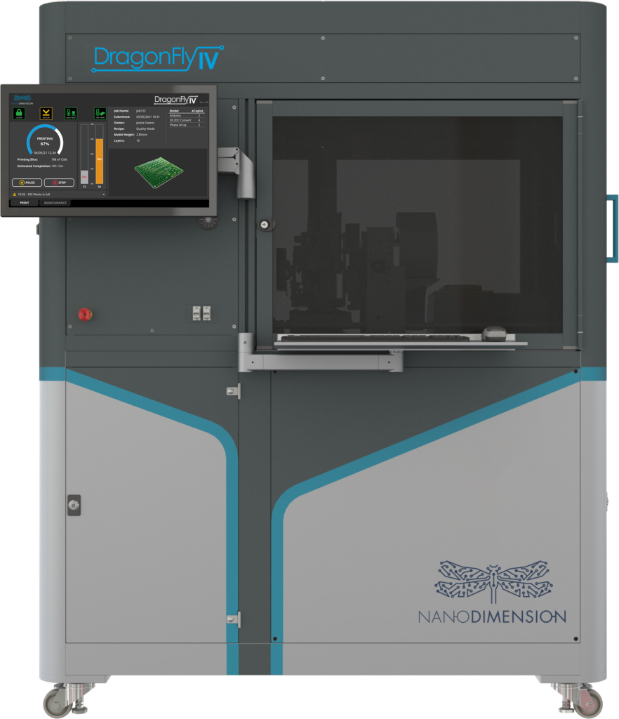
Nano Dimension DragonFly IV 3D-printer. Image courtesy of Nano Dimension.
The AME NanoLab@TTM facility will allow TTM customers and researchers to understand Nano Dimension’s additive manufacturing electronics (AME) technology in person. Using the firm’s latest DragonFly IV 3D printer and FLIGHT software, they will be able to see the AME workflow’s two steps: from design to 3D printed prototype circuit board. TTM has three DragonFly systems at the center already and will work hand-in-hand with customers as they explore the creation of electronic devices for a variety of industries, from military to medical.
“3-D printed electronics are rapidly evolving, delivering a step-change in electronics manufacturing,” said Sean Patterson, president of Americas, Nano Dimension. “With this industry-leading partnership, we’re launching our first AME NanoLab Network site. Our goal is to align roadmaps, research, and development to support TTM and their original equipment manufacturers, which will provide a better understanding of their use cases and materials requirements. As a result, customers will now be able to more easily explore the 3-D space for Hi-PEDs, while also reducing environmental impact in electronics manufacturing.”
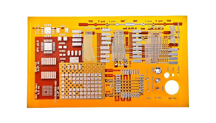
A 3D printed circuit board made with Nano Dimension technology. Image courtesy of Nano Dimension.
TTM is currently focused on “high-growth” markets and its investment in NanoDimension equipment demonstrates a forward-thinking approach to PCB design and production. Though the technology isn’t quite ready to produce chips for iPhones, it is a viable method for PCB prototyping. With all of Nano Dimension’s acquisitions, it’s possible that it will be able to perform more advanced electronics fabrication in the not-too-distant future, however.
As we noted in our article on the possibility of 3D printing an iPhone, the electronics 3D printing market is advancing quickly, with Optomec’s Aerosol Jet technology already being used to mass produce antennas for mobile phones as early as 2016. Because of the sensitive nature of electronics 3D printing, both due to the military applications and possible use by massive companies like Apple and Google, much of this advancement may be happening behind the scenes. That isn’t to say that it will break out into the public eye soon, but that we can assume that its progress is greater than what is made public.
This is described as the first AME NanoLab being established by the company, which has a goal of opening a network of such facilities. Together, the businesses hope to create specifications related to electronics 3D printing in the U.S., which would, of course, be necessary going forward as the technology evolves.
Subscribe to Our Email Newsletter
Stay up-to-date on all the latest news from the 3D printing industry and receive information and offers from third party vendors.
Print Services
Upload your 3D Models and get them printed quickly and efficiently.


You May Also Like
How the World’s Most Advanced Tech Companies Are Using 3D Printing
3D printing has been around for decades. For most of that time, it was a prototyping tool. Engineers used it to check if a design looked right before spending money...
The New Dental Lab: “Three Technicians Can Handle a Hundred Arches,” Says Digital Dentistry Expert Josh Jakson
Josh Jakson’s path into digital dentistry started long before he had a job title. He grew up around it. His father, a Polish immigrant, started the family’s dental laboratory in...
Why Beam Control Could Redefine the Future of EB-PBF
In Part 1, Ulf Lindhe examined how advances in beam control, point melting strategies, and process monitoring are changing the way engineers think about electron beam powder bed fusion (EB-PBF)....
Additive Manufacturing at a Crossroads
Additive manufacturing is at a crossroads. Simultaneously, we find ourselves between certain very different modalities, applications, and industries. Rather than being able to explore them all, companies will now have...