Proper 3D Printing Orientation and Technique Can Introduce Dielectric Strength Anisotropy into Insulator Components


3D printing has been applied to multiple projects across the various branches of the US military. However, before the technology can be used for more critical applications, some of its issues and imperfections still need to be better understood and conquered. The Air Force Research Lab (AFRL), headquartered at Wright-Patterson Air Force Base (WPAFB) near Dayton, Ohio, works to demystify the technology, and figure out how to apply it to various projects, such as cost-efficient solar cells and silicon chips.
The 3D printing industry has seen plenty of advancement over the last ten years, and allows for the manufacturing of dielectric insulators with highly complex geometries. But, something that causes problems with high voltage electrical generation and distribution systems is stress from the electric field on the dielectric insulating components, like bushings, which can cause dielectric breakdown events that damage those components and reduce the system lifetime.
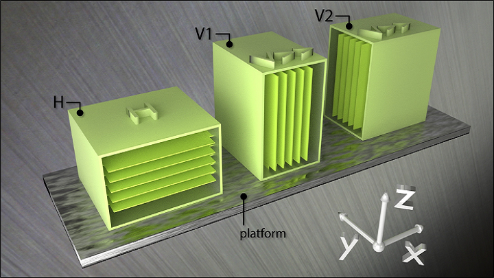
Schematic representation of sample coupon assemblies 3D printed in the H, V1, and V2 configurations.
At the moment, there isn’t a lot of bulk dielectric strength data available for many 3D printing materials, which can limit their use when it may not be necessary to do so. We need to learn more about the limitations of 3D printed parts that result specifically from the given printing method before widespread use of 3D printed dielectric insulators in high field environments can commence. Further research will also help guide development of new 3D printing systems and materials that are well-suited for creating parts for these applications.
AFRL set out to do just that, and together with researchers from the AFRL located at New Mexico’s Kirtland AFB, the Aramco Research Center in Boston, and UES, Inc., published a paper, titled “Dielectric strength heterogeneity associated with printing orientation in additively manufacturing polymer materials,” in the Additive Manufacturing journal.
The abstract reads, “Anisotropy in dielectric properties can have deleterious effects in structures intended for use in high-field environments. We show that dielectric anisotropy is introduced into parts fabricated using additive manufacturing techniques based on the orientation in which the part is printed. Dielectric strength testing data, based on the ASTM D149 standard, are presented for samples fabricated using the polymer jetting (PolyJet), stereolithography(SLA), fused deposition modeling (FDM), and selective laser sintering (SLS) additive manufacturing techniques. Each unique printing direction available, based on the printing method, was examined in turn. Each printing technique was found to introduce anisotropic dielectric properties within the sample coupons that were a function of the original orientation in which the part was printed, and the direction of structural susceptibility was found to be print-method dependent. Differences in dielectric strength for coupons printed in different orientations were found to exceed 70% for some combinations of printing technique and polymer.”
The researchers explained that the durability and size of insulators can be better optimized, which increases the reliability of the high voltage system and lowers component costs, by being careful in choosing their geometry. The data they collected in their study illustrates that dielectric strength anisotropy can be introduced into a 3D printed structure by picking the correct print orientation in respect to the build platform.
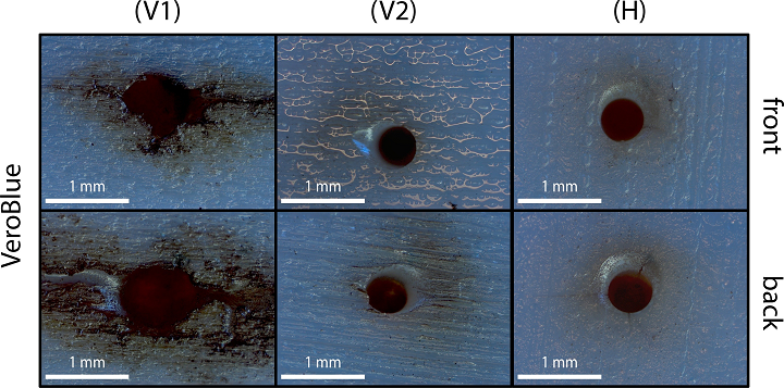
Post-failure microscopy images of VeroBlue samples showing the location of high voltage dielectric failure. The image set contains front and back photos from a failed (V1), (V2), and (H) coupon, tested according to the ASTM D149 Standard. Damage observable in this image set is representative of damage present after dielectric failure in all VeroBlue PolyJet sample coupons.
According to the paper, “The source of dielectric strength anisotropy is largely a consequence of the printing technique employed. Some printing techniques impart susceptibility to dielectric failure based on incomplete curing of starting materials and others through the introduction of structural microdomains or voids that can impart susceptibility to dielectric breakdown to the printed part.”

Dielectric strength testing results for 1 mm thick SLA-printed samples.
For their study, the team discussed dielectric failure mechanisms, and also examined the dielectric breakdown of model test structures (coupons) manufactured using four of the most common methods of 3D printing: PolyJet, SLA, SLS, and FDM.
The results showed that the test coupons 3D printed using SLA technology degree of dielectric strength heterogeneity was found to be smallest in the SLA coupons. The “(V) orientation yielding the highest dielectric strength and the (H) orientations exhibiting dielectric strength reductions of 8.3 and 16.1% for WaterShed 11122 and ProtoGen.”
As expected with FDM, the difference “in dielectric strength between structures printed in the (H) and (V1/V2) orientations was found to be greater than 73% in the ABS-M30 samples and greater than 23% in the ABS-M30i samples.” SLS coupons had reduced dialectic strength in “(V) orientation, compared to (H) oriented samples. This difference was approximately 31% for the DuraForm HST structures and 16% for the Nylon EX structures.”
According to the paper, PolyJet “showed a dramatic reduction in dielectric strength in the (V1) orientation, compared to the (V2) and (H) orientations. For structures printed using the VeroBlue photopolymer, this difference was greater than 50%; the difference exceeded 70% for samples printed using the VeroAmber photopolymer.”
Non uniform curing was attributed to cause these issues in Polyjet due to printhead placement vis a vis laser, while in SLA the issue was anisotropic curing with different laser pathways occurring in different areas of the part. In SLS, ” Pore networks formed as an artifact of the printing process are likely the strongest contributor to observed differences” while in FDM a Void Layergaps are a probable cause.
Co-authors of the paper are Brad W. Hoff, Sabrina S. Maestas, Steven C. Hayden, Daniel J. Harrigan, Rachael O. Grudt, Michele L. Ostraat, John C. Horwath, and Serhiy Leontsev.
Discuss this story and other 3D printing topics at 3DPrintBoard.com or share your thoughts in the Facebook comments below.
Subscribe to Our Email Newsletter
Stay up-to-date on all the latest news from the 3D printing industry and receive information and offers from third party vendors.
Print Services
Upload your 3D Models and get them printed quickly and efficiently.


You May Also Like
Australia’s AMCRC Funds Titanium 3D Printing R&D
In terms of the global economy’s presently existing state, there is no realistic path to economic resilience that doesn’t start with critical minerals security. This is a problem for pretty...
3DPOD 305: Automating AM with Grenzebach’s Oliver Elbert
Oliver Elbert‘s over ten years in additive manufacturing have been spent automating LPBF. For large, high-volume, or critical parts, Grenzebach has provided custom automation solutions. Depowdering, powder handling, sieving, heat...
AMPulse Asia: Chinese IPOs, Defense Deals, and Dental 3D Printing Lead APAC Roundup
The second half of June brought a wave of additive manufacturing activity across China, Japan, South Korea, India, and Australia. From Chinese IPOs and funding rounds to defense, aerospace, construction,...
Austal, Curtin University and AMCRC Work on R&D Together
Australia’s Additive Manufacturing Cooperative Research Centre (AMCRC) works with 70 industry partners to deliver collaborative R&D projects. They also work on workforce development and technology transfer. It’s kind of analogous...