How Nano 3D Electronics Printing Will Drive the Internet of Things

Plastic printed electronics will be dominated by 3D printing technologies, and they’ll be critical to the development of what researchers are calling the Internet of Things.
The Internet of Things (IoT) is essentially an interconnection of uniquely identifiable, embedded computing devices inside the existing framework of the Internet. IoT promises advanced connectivity of devices, systems, and services to bring automation to nearly every field of endeavor. The IoT concept includes connectivity for devices like human heart monitor implants, biochips in farm animals, field operation tools for police and firemen, and even built-in sensor packages for automobiles and kitchen appliances. Think smart thermostat systems and wifi-enabled washers and dryers.
Some pundits project that by the year 2020, there will be 26 billion devices on the Internet of Things.
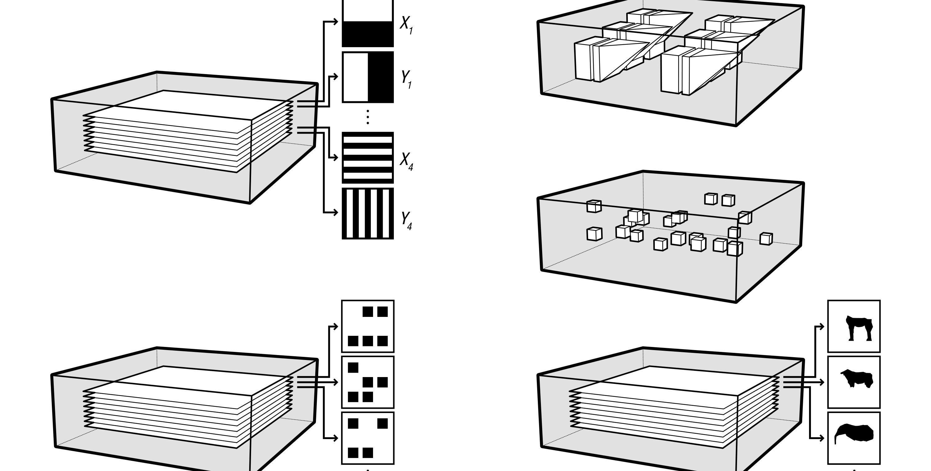
3D printed InfraStructs
Researchers at Belgian nanotechnology research center imec have used inkjet printing technology to output a transistor logic board which included a mind-boggling almost 3,400 circuits. It measured only 2 x 2 cm and ran at a speedy 6 Hz.

Dr. Janusz Bryzek
They’re calling such plastic circuits an “exponential technology,” and Dr. Janusz Bryzek, the man who founded the Trillion Sensor movement and has co-founded some nine separate companies dedicated to MEMS technologies, believes printable transistor processes will one day be used to print transistors with the power of today’s chips on a 3D printer.
Bryzek adds that traditional semiconductor companies will undergo a violent upheaval as 3D printing is adopted.
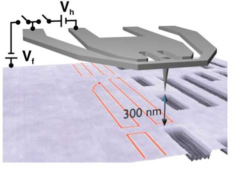
Researchers at the IBM Zurich lab have already used an atomic force microscope to create 3D patterns on the nanometer-scale on organic material, and they used such patterned organic material as a ‘mask’ to create circuits.
Technologists see a day when the dimensions of plastic printed electronics will become smaller at an exponential rate and that could lead, within 10 years, to plastic circuits which operate at performance levels equal to those of silicon circuits today.
And the key is that plastic electronic circuits cost much less to build than a like silicon-based device.
 Scientists have also arrived at a method of 3D printing unique tags they call InfraStructs inside objects as they’re being printed. The technology is driven by terahertz imaging, a radiation band technique which utilizes wavelengths in the submillimeter range between microwave and infrared on the electromagnetic spectrum. Such wavelengths can penetrate paper, textiles, and plastics — and they can do it without harming living tissue. Researchers at Carnegie Mellon University and Microsoft Research have already used 3D printed InfraStruct tags to identify objects and terahertz imaging processes to decode the information in them.
The manufacturing processes using 3D printing don’t require vacuums or particularly high temperatures, and they can be printed with less finicky liquids and materials.
“Plastic circuits could end up having perhaps 1/1,000th the cost-per-area of the equivalent silicon device,” Bryzek says.

He adds that plastic printed transistors will function as keys to creating wearable electronics and innovations for the Internet of Things.
A 3D printed nanoshape can serve as a mold — or as the circuit itself — using graphene-based construction techniques.
Consider that the conventional, electron-beam lithography equipment used to manufacture semiconductors costs from $1.5 million and run to $30 million each, and a system capable of 3D printing electronics on the nano scale might run $500,000, and the future of the IoT becomes clear.
What uses can you envision for 3D printing to drive the Internet of Things? Tell us about applications you’ve seen and let us know about any work being done in the field in the 3D Printing Internet of Things forum thread on 3DPB.com.
Subscribe to Our Email Newsletter
Stay up-to-date on all the latest news from the 3D printing industry and receive information and offers from third party vendors.
Print Services
Upload your 3D Models and get them printed quickly and efficiently.













You May Also Like
Stratasys Showcases 3D Printed Automotive Applications & New Printer at IMTS 2026
Just ahead of last week’s International Manufacturing Technology Show (IMTS) in Chicago, Stratasys launched the F870, a new large-format, production-grade FDM 3D printing platform designed to drive industrial manufacturing at...
3D Printing Financials: $28M in China, U.S. Deals and a Metal AM Comeback
Money continues to go into additive manufacturing (AM). From a $30 million raise for a Chinese metal 3D printing company to new funding for naval AM and a European company...
Stratasys Wins $27.6M in Patent Case Against Bambu Lab; Bambu Challenges Verdict
Update, September 21, 2026: This article has been updated with a statement from Bambu Lab responding to the verdict, along with additional information about the company’s ongoing patent challenges against...
AMAsia Pulse: AM Investment Picks Up Across Asia-Pacific
The first half of September brought fresh investment and expansion activity across Asia-Pacific’s additive manufacturing sector. China’s Xinjinghe secured funding for an aerospace AM hub, South Korea’s Lincsolution outlined plans...