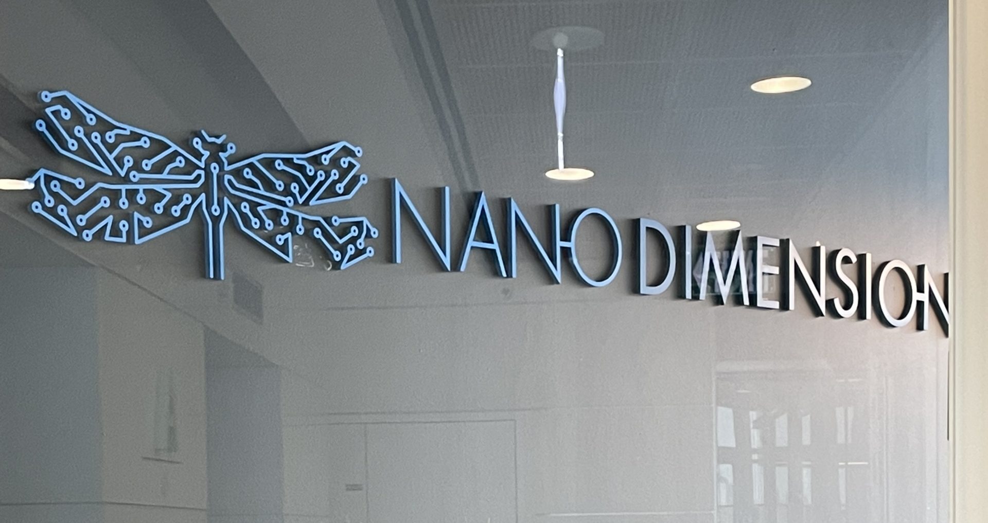
A Trip to Nano Dimension HQ: Electronics 3D Printing Live and In-Person

Earlier this month, I traveled to Israel for a 3D printing event and several site visits. The final company I had the opportunity to see while in the Tel Aviv area was printed circuit board (PCB) leader Nano Dimension.
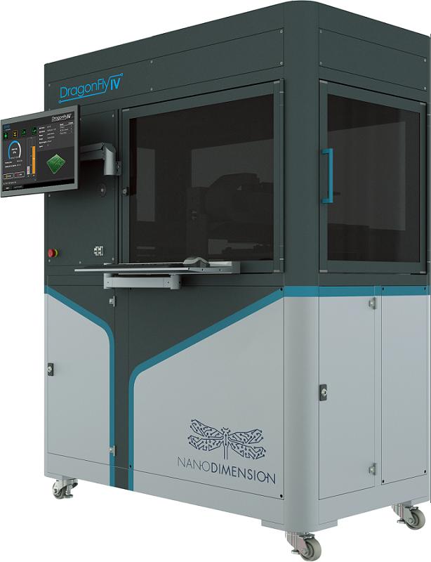
When I first began writing for 3DPrint.com in 2016, Nano Dimension was a frequent topic. It announced customer after customer for its newly released DragonFly 2020, touted as the world’s first desktop electronics 3D printer. The company has been going strong ever since. It released its industrial DragonFly 2020 Pro 3D printer in 2017. It opened its first 3D printed electronics service bureau a year later. And it continued to announce advantageous partnerships. Most recently, Nano Dimension unveiled its DragonFly IV this fall, and I was excited to see it for myself at the company’s Israeli headquarters in Ness Ziona.
-

- Photos by Sarah Saunders for 3DPrint.com
I was met in the reception area by Julien Lederman, Director of Corporate Development for Nano Dimension, who then took me on a quick tour of the space. We started with the area that houses Nano Dimension’s Additively Manufactured Electronics (AME) systems. These, as Lederman explained, have “effectively two materials in the same printer at the same time.” These include both Nano Dimensions’ proprietary conductive and nonconductive materials, developed in a materials area located on the first floor of the building.
The second floor is where the company’s Fabrica Group (formerly Nanofabrica) 3D printers are. Last year, Nano Dimension acquired and rebranded the microscale AM company, which specializes in precise, tiny 3D prints with features down to 1 micron in size. This was the company’s first acquisition in the AM sector, and as Lederman explained, there are plans for Nano Dimension to acquire more AM companies and “become a dominant player.”
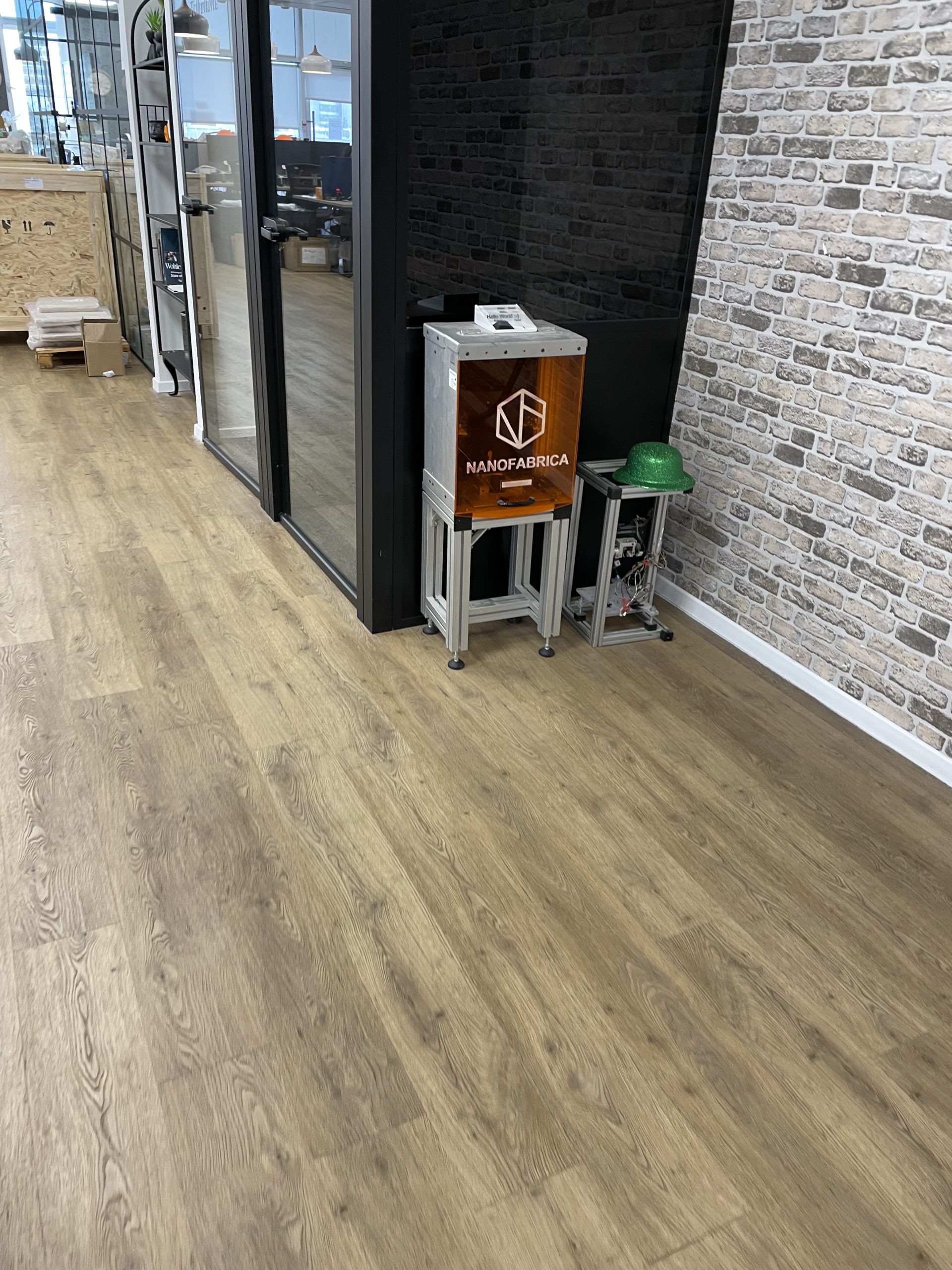
Photo by Sarah Saunders for 3DPrint.com
Though it was the first in the AM space, Nanofabrica was certainly not the company’s first ever acquisition. In fact, the same week that Nano Dimension purchased Nanofabrica, it also acquired DeepCube, a real-time, deep machine learning, AI company. By integrating DeepCube’s software platform into its solutions, and those of its other acquired companies, Nano Dimension can close the loop in smart industrial solutions and “execute machine learning on the fly.”
“So, on top of the revenue we gain from these leading companies in the Western world, we have a complementary technology for our AME solutions,” Lederman told me.
I asked Lederman how micro 3D printing, and other acquisitions, fit into Nano Dimension’s larger tech strategy. He filled me in, starting with electronics company Essemtec, which develops technology for pick-and-place technology. Nano Dimension sells Essemtec’s electronic manufacturing services (EMS) to its assembly customers. Additionally, as Nano Dimension fabricates its PCBs layer by layer, Essemtec’s solutions make it possible to embed components inside and on top of the PCBs.

Photo by Sarah Saunders for 3DPrint.com
Nano Dimension also acquired UK-based company GIS (Global Inkjet Systems), which is focused on inkjet technology—the “primary tech in our AME solutions.” GIS has hundreds of global customers in the 3D printing and graphic arts sectors, and sells ink delivery systems, controller electronics for inkjet printheads, and the software that “orchestrates all these components together.” This acquired company has significant revenue, which makes it an ideal acquisition. However, its complementary technology was the real draw here, as Nano Dimension can maximize its own inkjet process used in its AME solutions.
Hanan Gino, CPO and Head of Strategic M&A at Nano Dimension, joined us then, and he and Lederman explained to me that the company’s portfolio offers a proof of concept for academia in regards to AME. According to the executive, the firm’s next-generation systems will be focused on prototyping first, with functional PCB manufacturing coming later. The end goal is to sell the solution to manufacturers producing PCBs. In regards to its strategic acquisitions, Nano Dimension looks for technology that complements its own AME solution, in addition to equipment vendors in the same domain, “which means horizontal integration.”
“We also look for companies who will give us the presence in the right market, and companies in material development, as everything we do is based around this. So, that’s the scope of what we’re looking for.”
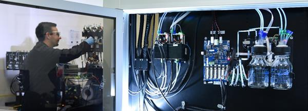
Global Inkjet Systems showing Inkjet System Components in a laboratory environment. Image courtesy of Nano Dimesnion.
Gino explained that Nano Dimension has a “unique operation,” and that it’s growing fast. When he joined the team a year ago, there were 80 employees, but after four acquisitions, they’re close to 500.
“We built the company from the bottom up” he told me. “We have great technology, and a real challenge—we want to revolutionize the electronics industry.
“With the graphic arts domain, and 2D printing on paper…the eye is very sensitive. And then you have 3D printing, which is 3D but not really functional. When you go to AME, you add the functionality dimension. It should be 3D and also functional. So, it’s very, very complex.”
Nano Dimension also invests a lot in different feedstocks for different applications, because the company believes each application will require a unique material. Gino said that Nano Dimension works with 20 external material companies to develop additional feedstocks, and that the company also develops two main families of inks—conductive and electric—in-house.
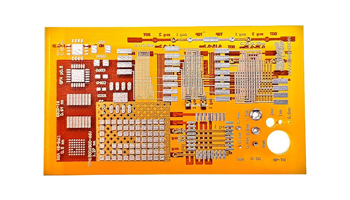
A 3D printed circuit board made with Nano Dimension technology. Image courtesy of Nano Dimension.
I asked how many PCBs the DragonFly can make in a single print process. Gino said it depended on how many materials were needed, as well as the complexity of the product and the number of layers required. But he was able to give me a ballpark figure and said it can take “tens of hours to fabricate this kind of product.”
“That’s the current solution we have, but we are in the advanced stages of developing our next-generation product. So, we’re hoping to reduce that number,” he said. “The target is to make a very large PCB in a very few hours.”
Gino explained that for one of their customers, which he wasn’t allowed to name but assured me had plenty of available revenue, Nano Dimension replaced its entire PCB lines—which used to consist of 70-100 stages—with a single solution. This was helped by the fact that the company has several R&D centers, with the main one in Israel, another in Boston, and one in Munich. This helps shorten the time to market.
“In the last year, we’ve become a totally different company,” Gino said. “We’re not young, but since our CEO raised the money, we have the capital and we can use it to acquire companies.”
He said that Nano Dimension also has enough revenue to be disruptive, and has recruited people from some other big-name companies, like Amazon, 3D Systems, and PCB manufacturing company TTM.
“We are equipped with the right people and the right technology,” Gino said.
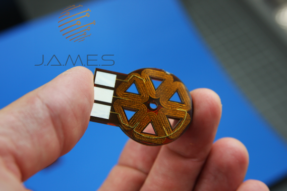
Speaking of TTM, it’s the leading PCB manufacturer in the western world, according to Gino. It is also one of Nano Dimension’s partners, having purchased three of its DragonFly systems. He also mentioned Jetted Additively Manufactured Electronics Sources (JAMES). JAMES is a joint venture with Hensoldt AG, a market leader in civilian and military sensor solutions and defense and security electronics. The goal behind this is to develop a crowdsourcing platform in order to get more people involved in 3D design. Nano Dimension also offers the AME Academy, which is a platform that offers different types of webinars that champion new types of electronics design.
Before I left, Gino relayed some crucial specifics of Nano Dimension’s technology, first noting that strength and weight ratios, and internal architectures, are talked about a lot with AME.
“AME is different from the conventional PCB manufacturing in multiple aspects: it is eco-friendly without any toxic material, it simplifies and digitizes manufacturing processes, and it allows for previously unprecedented geometries and complex devices,” he explained. “With AME, it’s effectively about a multi-material, multi-layer 3D, end-to-end solution that generates the entire circuits in one step, including substrate, conductive traces, and passive components.”
He explained that you are “bound by right angles of connections in the Z dimension and by physical limitations of a PCB” with traditional printed circuit boards, but that you don’t have this limitation with AME.
“Traditional PCB manufacturing isn’t really a 3D structure, it is 2.5D,” Gino explained. “Multiple 2D layers are manufactured separately and then connected through the plated holes (vias) to each other.”
Gino told me that the biggest pain points in traditional PCB manufacturing are holes drilling, holes plating, and the registration between layers. These issues can be overcome with AME because Nano Dimension doesn’t drill holes.
“We print just the pattern itself, we plate the holes using additive manufacturing technology and we print all layers on the same printer, thus we do not face registration problems.
“With our AME tech, we enable electronic designers to utilize and maximize the power of the 3D.”
Gino said with Nano Dimension’s solution, “the pads on a PCB can be connected from any point to another directly,” instead of only through the vias, which are holes drilled to connect conductors on different layers.
“It’s like drawing an electronic picture in free space,” he concluded.
To see Nano Dimension’s PCB technology for yourself, come visit the company at Rapid.Tech 3D in Erfurt, Germany, and at RAPID + TCT in Detroit, Michigan, May 17-19.
Subscribe to Our Email Newsletter
Stay up-to-date on all the latest news from the 3D printing industry and receive information and offers from third party vendors.
You May Also Like
GREENFILL3D 3D Prints Sustainable Interior Solutions for Stretch Ceilings
Polish startup GREENFILL3D has previously produced sustainable in-store displays, plant markers, and lamps using sustainable materials and desktop 3D printers. I appreciate GREENFILL3D for its use of low-cost material extrusion...
3D Printing News Unpeeled: A $3000 SLS System, Construction Subsidies and Parameters
The Housing Affordability Crisis is one of Canadian President Trudeau’s biggest issues. Now the government has made subsidies available, including scaling new technologies, 3D printed housing and libraries of reapproved...
3D Printing News Briefs, April 6, 2024: Depowdering, Cybertruck Door Handles, & More
In today’s 3D Printing News Briefs, ioTech’s digital manufacturing CLAD technology is opening up opportunities for microelectronics and additive manufacturing. Hexagon and Raytheon Technologies commercially released the Simufact Additive Process...
“Bundled Light” Enables High Quality Plastic 3D Printing from LEAM
Naturally, we expect current 3D printing methods to continuously improve, but it continues to do so in the most surprising ways. The latest development comes from LEAM, a startup spun...