Spain: Influences of Parameters & Post-Processing on Conductive 3D Printed Parts


Researchers in Spain explore complexities of parameters in digital fabrication, and properties in materials and parts, releasing their findings in ‘Influence of Manufacturing Parameters and Post Processing on the Electrical Conductivity of Extrusion-Based 3D Printed Nanocomposite Parts.’
In this study, the authors are concerned with the effects of extrusion-based additive manufacturing processes on graphene nanoplatelets, including post-processing efforts. Conductivity in materials for 3D printing continues to be a growing area of interest whether seeking greater functionality, compatibility with sensors, antennas, or smart textiles. Such materials may be critical in applications for automotive, aerospace, energy, and more, as well as working well in combination with other composites.
“Particularly, carbon-based nanoreinforcement, such as carbon nanotubes (CNTs) and graphene nanoplatelets (GNPs), has been widely investigated. Percolation thresholds for GNPs-based nanocomposites have been published to be between 1 to 10 wt %, depending on the lateral dimensions of the nanoplatelets and their thickness, as well as the dispersion degree and orientation,” stated the researchers.
For this study, the researchers used GNP/ABS nanocomposite pellets with a GNP content of 15 wt %, extruded using the Noztek Touch. Extruded filaments demonstrating high conductivity were printed on a Prusa i3 3D printer.
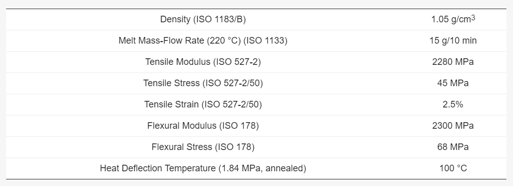
Acrylonitrile butadiene styrene ABS properties.
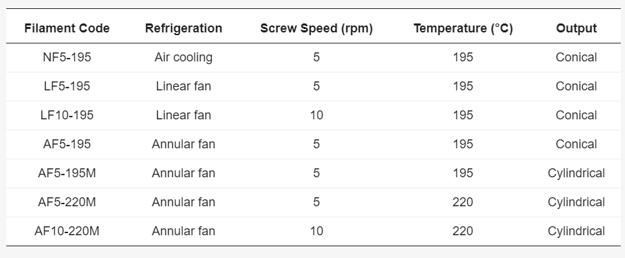
Operational parameters for filament extrusion.
3D printed samples measured 10 × 10 × 10 mm3, and varying thicknesses and widths for extrusion were analyzed for studying the effects of conductivity on the fabricated parts. The samples were also painted silver to decrease contact resistance, with electrical resistance measuring along the x, y, and z axes.
Operational parameters for 3D printed parts.
Post processing consisted of several different processes, to include vapor polishing with acetone, plasma post processing, and neosanding.

Samples for measurement of (a,c) volume and (b,d) surface electrical conductivity of: (a,b) filaments and (c,d) 3D printed parts (1 index: schematic representation; 2 index: real part)
The researchers noted that in every case, conductivity of the filaments was ‘more than one order of magnitude lower than the volume electrical conductivity,’ caused by reduced filament diameters which resulted in increased surface-to-cross-section ratios. The AF10-220M filament exhibited the greatest uniformity, and ultimately, was used for fabrication of cubic parts with different thickness and widths.
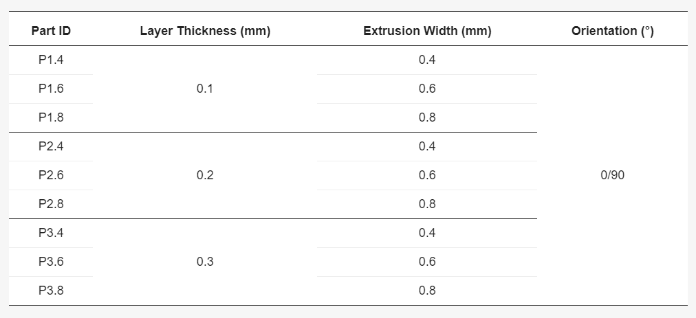
Optical micrographs of the surface of 3D printed parts: (a) P1.4, (b) P1.6, (c) P1.8, (d) P2.4, (e) P2.6, (f) P2.8, (g) P3.4, (h) P3.6 and (i) P3.8 (t = layer thickness, w = extrusion width)
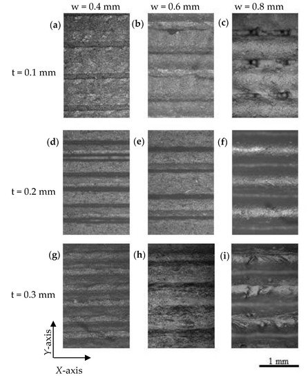
Optical micrographs of the layers thickness of 3D printed parts: (a) P1.4, (b) P1.6, (c) P1.8, (d) P2.4, (e) P2.6, (f) P2.8, (g) P3.4, (h) P3.6 and (i) P3.8 (t = layer thickness, w = extrusion width)
The research team also noted that volume and surface conductivity were lower in comparison to the filament conductivity.
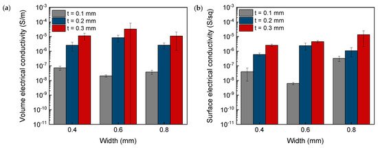
Volume (along Z-axis) (a) and surface (b) electrical conductivity (along X-axis) of 3D printed parts
“The operational parameters in 3D printing have also shown to be crucial to maximize the electrical conductivity. In the absence of defects, the volume electrical conductivity of 3D printed parts is enhanced by increasing the printing layer thickness and extrusion width. This improvement is caused by two effects. On the one hand, the number of layers to achieve the same part height is lower when using higher printing layer thicknesses, thus leading to reduced electrical resistance. On the other hand, the higher the layer thickness and extrusion width are, the greater the cross-section area of the printed lines, resulting in a lower electrical resistance,” concluded the researchers.
“The effect of different post processing of 3D printed parts in morphology and surface electrical conductivity was also analyzed. While acetone vapor polishing induced a diminution in surface electrical conductivity close to one order of magnitude; enhancement of the electrical conductivity along the X-axis was obtained for plasma treated parts. Neosanding post processed samples showed surface electrical conductivities in the range of 10−7–10−5 S/sq. This variability demonstrated that precision is a key factor to have reproducible results in this novel technique.”
What do you think of this news? Let us know your thoughts! Join the discussion of this and other 3D printing topics at 3DPrintBoard.com.
[Source / Images: ‘Influence of Manufacturing Parameters and Post Processing on the Electrical Conductivity of Extrusion-Based 3D Printed Nanocomposite Parts’]Subscribe to Our Email Newsletter
Stay up-to-date on all the latest news from the 3D printing industry and receive information and offers from third party vendors.
Print Services
Upload your 3D Models and get them printed quickly and efficiently.


You May Also Like
The SLS Market, Game of Trucks: Part 2
With the release of the new HP 1200 and the Formlabs X1, we can see real competition from very different segments. From several million dollars to just $20,000, the laser...
3D Printing News Briefs, May 2, 2026: Soft Robots, Agricultural Waste, & More
In this weekend’s 3D Printing News Briefs, we’ll start off with a multi-laser metal powder bed fusion 3D printer and post-processing news. We’ll end with research into soft robotics and...
3D Printing News Briefs, April 4, 2026: 3D Printed Food, Cocoa Press, & More
We’re starting off with 3D printed food in this weekend’s 3D Printing News Briefs, followed by some business news about Cocoa Press. Then we’ll move onto a metal additive manufacturing...
3D Printing News Briefs, March 28, 2026: TCT Asia, Distribution Agreement, FDA Clearance
We’re starting 3D Printing News Briefs this weekend with some news out of TCT Asia, and then moving on to a metal AM distribution agreement between MULTISTATION and WAAM3D. We’ll...