University of Sheffield: Comparative Research of SLM & EBM Additive Manufacturing with Tungsten

Jonathan Wright recently submitted a thesis to the Department of Materials Science and Engineering at The University of Sheffield, exploring 3D printing with tungsten, a rare metal. In ‘Additive Manufacturing of Tungsten via Selective Laser Melting and Electron Beam Melting,’ Wright details the potential for powder bed additive layer manufacturing (ALM) of pure tungsten, using both selective laser melting (SLM) and electron beam melting (EBM).
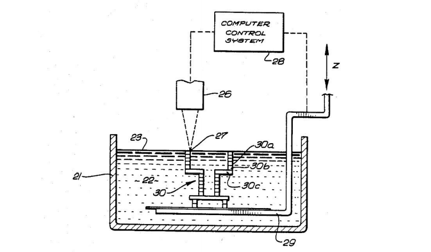
Referring to the layered approach of 3D printing or additive manufacturing, Wright chooses to encompass most of this technology as ALM, reminding us that Chuck Hull of 3D Systems fame was granted the patent in 1986 after he created stereolithography (SLA).

Schematic Diagram of the SLA Process. Diagram taken from ’Apparatus for production of three-dimensional objects by Stereolithography’
Patent application [1]
“An advantage of the ALM approach is the fact that no additional tooling is required for new components,” stated Wright. “This tool-less approach results in shorter lead times and reduced cost for new products.”
Users in a variety of industries today also enjoy major benefits such as less waste in material, greater savings on the bottom line, and the potential for environmentally friendly processes in some cases, whether powder-based, liquid-based, or solid deposition.

An overview of ALM processes and hardware (adapted from [6])
Tungsten, derived from wolframite ((Fe,Mn)WO4) and scheelite (CaWO4), not only has the lowest vapor pressure of any element but also offers a high melting point and the capability for being ‘drawn into fine wire.’ Used in lamp filaments and a variety of other applications today, it can be used in high temperatures or in cases where high density is required such as X-ray shielding.
Wright also explains that because of tungsten’s thermal properties, ‘low spluttering yield, and short activation decay time,’ it is also suitable for nuclear fusion experiments.
“Tungsten can be machined, (drilled, turned, milled, etc.) however this is difficult, requires expertise, and close adherence to ideal conditions,” states Wright. “Structures with greater complexity can be formed by Electrical Discharge Machining (EDM) overcoming some of these difficulties.”
Because there are challenges and limitations due to the chemical, physical, and mechanical makeup of tungsten, alloying is a consideration; however, Wright notes that a ‘huge number’ of alloys have been examined but not found to be important. So far, tungsten-rhenium alloys have been considered to show the greatest potential for improving ductility.
A general flow diagram for the hydrometallurgy of tungsten [62]

Renishaw SLM 125 System
For EBM processes, an Arcam S12 system was used.
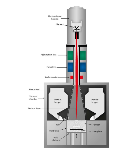
Schematic of ARCAM S12 EBM System. Image from arcam.com
Wright discovered that it was not possible to create tungsten parts without defects, and that beam power was one of the greatest reasons for porosity, with all samples exhibiting high levels at 200W and for 400W, the lowest.
“As porosity in tungsten samples produced via SLM was reduced the number of cracks was found to increase, this was also therefore a function of beam power,” explained Wright.
“Further work needs to be carried out on SLM of tungsten in order produce crack free parts. This may include an investigation of adding an external heat source. A heated environment is likely to reduce residual stresses and raise material above the DBTT.”
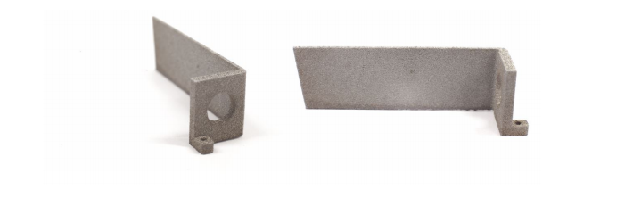
A tungsten Langmuir Probe manufactured via SLM. 25mm in length
In experimenting with fabrication of EBM samples, Wright was able to pinpoint the proper parameters for tungsten samples with low defects. He identified speed, current, and hatch spacing as playing a large role in porosity.
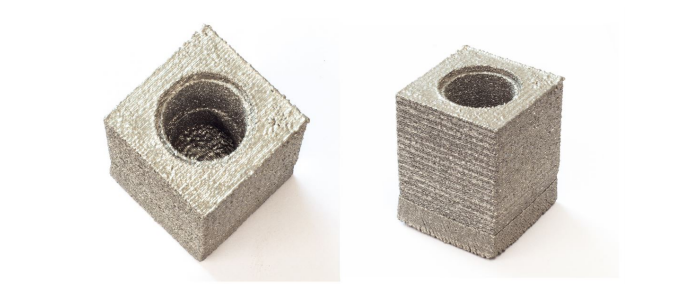
A tungsten mono-block manufactured via EBM. External dimensions of 20mm x 20mm x 25mm
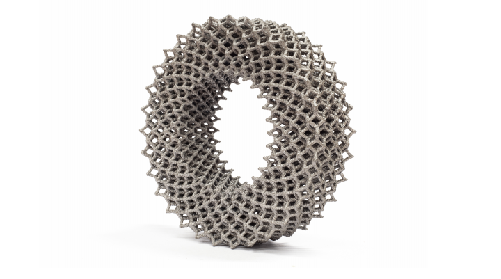
A tungsten lattice structure manufactured via EBM. External diameter: 80mm. Thickness: 20mm
“For the first time EBM of tungsten has been reported. Specifically, EBM was able to produce low porosity, crack free parts. EBM appears to the preferable manufacturing process due to its combination of a vacuum environment, high build temperatures and high beam power,” concluded Wright.
“Nonetheless, mechanical properties and geometric accuracy require further improvements before ALM can be used to manufacture tungsten for structural applications. For Applications where mechanical properties are non-critical and complex geometry is required, such as in x-ray collimation, the ALM techniques outlined here could provide a viable processing route.”
As researchers around the world continue to refine 3D printing and AM processes, tungsten is being investigated from examining its properties, to fabricating cutting tools, and large unalloyed parts.
What do you think of this news? Let us know your thoughts! Join the discussion of this and other 3D printing topics at 3DPrintBoard.com.
[Source / Images: ‘Additive Manufacturing of Tungsten via Selective Laser Melting and Electron Beam Melting’]Subscribe to Our Email Newsletter
Stay up-to-date on all the latest news from the 3D printing industry and receive information and offers from third party vendors.
You May Also Like
Human Remains Could Be Identified with the Help of Forensic 3D Printing
I’m still in awe at what additive technologies can accomplish, from creating alternative meats, automotive parts, shoe insoles, and surgical models, to giving faces to the lost. That is to...
3D Printing News Briefs, May 17, 2023: Stress-Resistant Alloy, 3D Printed Trophies, & More
In today’s 3D Printing News Briefs, we’re starting off with a little research, as materials scientists developed a 3D printing process that produces an extremely stress-resistant alloy. Moving on to...
On the Ground with COBOD Construction 3D Printing at Ohio State
This winter, The Ohio State University’s Center for Design and Manufacturing Excellence (CDME), which is one of the country’s largest additive research groups, received a COBOD BOD2 3D construction printer...
3D Printing Webinar & Event Roundup: April 2, 2023
You can breathe easy this week, because it will be much less hectic than last week, at least in terms of 3D printing webinars and events to attend! There will...