Cranfield University Researchers Use WAAM Process to Produce Large-Scale Parts in Unalloyed Tungsten
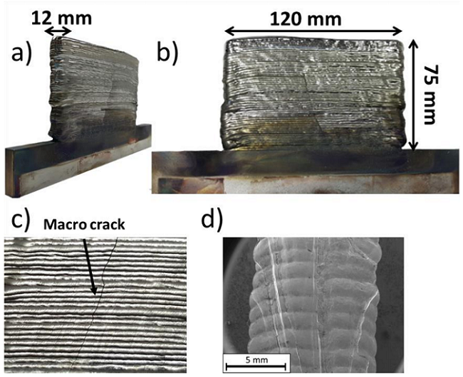
Large-scale unalloyed tungsten linear structure deposited via WAAM process (a-b). Picture of the fracture from the outer surface (c) and SEM picture of the fractured surface (d).
Cranfield University is continuing its work with Wire and arc additive manufacturing, or WAAM: a novel process that uses an electric arc as the heat source, and high-quality metal wire as the feedstock. A trio of researchers with the university’s Welding Engineering and Laser Processing Centre (WELPC) published a paper, titled “Development of Wire + Arc Additive Manufacturing for the production of large-scale unalloyed tungsten components,” which demonstrates that WAAM can produce large-scale parts in unalloyed tungsten by complete fusion. This is a possible alternative to using powder metallurgy for manufacturing tungsten.
The abstract reads, “The manufacturing of refractory-metals components presents some limitations induced by the materials’ characteristic low-temperature brittleness and high susceptibility to oxidation. Powder metallurgy is typically the manufacturing process of choice. Recently, Wire + Arc Additive Manufacturing has proven capable to produce fully-dense large-scale metal parts at relatively low cost, by using high-quality wire as feedstock. In this study, this technique has been used for the production of large-scale tungsten linear structures. The orientation of the wire feeding has been studied and optimised to obtain defect-free tungsten deposits. In particular, front wire feeding eliminated the occurrence of pores and micro-cracks, when compared to side wire feeding. The microstructure, the occurrence of defects and their relationship with the deposition process have also been discussed. Despite the repetitive thermal cycles and the inherent brittleness of the material, the as-deposited structures were free from internal cracks and the layer dimensions were stable during the entire deposition process. This enabled the production of a relatively large-scale component, with the dimension of 210 x 75 x 12 mm.”
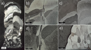
Microstructure of the linear structure deposited using front wire feeding (a). Details of elongated grains at the center of the structure (b, d). Detail of microstructure of the upper part (c) and base of the linear structure (e).
Tungsten is a major candidate for manufacturing components in the energy sector, which require materials with high heat resistance, neutron load-capacity, and excellent mechanical properties. Because tungsten has the highest melting point of all metals, along with low tritium retention, relatively high thermal conductivity and density, and good resistance to sputtering and erosion, it can be used in in future fusion reactors as a plasma-facing material. But, due to the metal’s high recrystallization temperature and low fracture toughness, it’s not that easy to manufacture tungsten components.
“Currently, there are three main manufacturing operations that are being studied, when referring to tungsten components for nuclear fusion environment: the industrial production of large-scale components; the joining of these parts with other materials; and their efficient repair and maintenance,” the researchers explained, noting that additive manufacturing can be used to manufacture the alloy.
“AM could definitely address some of the manufacturing issues related to tungsten components, and possibly enable the development of new designs approaches.”
WAAM is able to directly fabricate large, fully-dense, metallic, near-net-shape components at a higher deposition rate than other metal 3D printing processes. So the team wanted to apply WAAM for the first time to unalloyed tungsten, paying special attention to creating large-scale components that were free of defects.
“The study and monitoring of the metal transfer, and the characterisation from the microstructural point of view are discussed,” the researchers wrote. “A structure of realistic scale has also been produced to understand the issues related to scaling up, and ultimately assess the feasibility of WAAM’s implementation as an innovative way to produce unalloyed tungsten parts.”
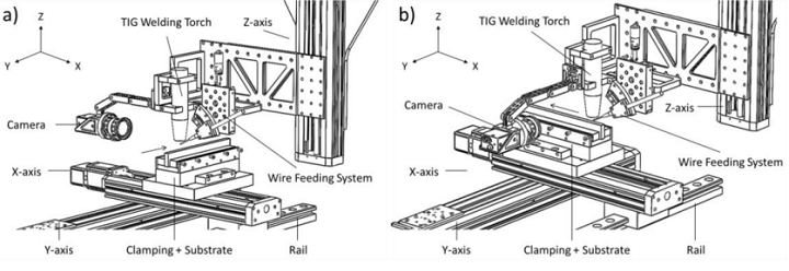
Setup for development of WAAM process for unalloyed tungsten when using side wire (a) and front wire feeding (b).
The above image depicts the apparatus the team used for deposition. For the side wire and front wire feeding configurations, tungsten layers were deposited progressively onto the substrate, in a constant direction, with a single bead. The cross-section perpendicular to the direction of the deposition was ground up, polished, and etched, in order to examine defects and the microstructure. Once the researchers landed on the optimal parameters, they used the WAAM process to build a tungsten wall that was 120 mm in length, 75 mm high, and 12 mm thick.
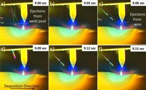
While there were no signs of spatter during deposition for the front wire feeding, there were some spattered particles during the side wire feeding configuration, mainly caused by two main ejection mechanisms.
“The droplets or macroscopic mass losses, localised predominantly along the melted surface, arose because of the Kelvin–Helmholtz instability,” the researchers explained. “This phenomenon occurs when there is a difference in velocity across the interface between two fluids. Furthermore, it has been reported that the Kelvin–Helmholtz instability can also lead to the evolution of shock waves along the surface of the fluid causing a breakup of the melt surface into droplets.”
This lack of spattered particles on the front wire feeding directly correlates to a lack of fusion and pores in the structure, so it’s important to avoid spatters if you want to keep the WAAM-deposited tungsten structure strong.
With both side- and front-fed deposit, the microstructure contained fine equiaxed grains near the bottom layers, with larger, more coarse grains near the top. The team explained that the tungsten’s high thermal conductivity at room temperature, along with rapid solidification, promoted the equiaxed grains.
“This possibly represents the first fully-dense large-scale structure in unalloyed tungsten produced using AM. The unique aspects of this structure were the absence of any large network of grain boundary cracks within the volume deposited, the almost absence of discolouration and oxidation from the fusion process, and the consistency in the layers’ geometry,” the team stated.
The study showed that, while WAAM technology can produce “large-scale refractory metal components by complete fusion” out of high-purity tungsten, the orientation of the wire feeding can majorly influence the deposit’s microstructure, along with creating structural defects and pores.
Co-authors of the paper are G. Marinelli, F. Martinaa, S. Gangulya, and S. Williams.
Discuss this and other 3D printing topics at 3DPrintBoard.com or share your thoughts below.
Subscribe to Our Email Newsletter
Stay up-to-date on all the latest news from the 3D printing industry and receive information and offers from third party vendors.
Print Services
Upload your 3D Models and get them printed quickly and efficiently.
You May Also Like
3D Printing News Briefs, June 11, 2025: Sustainability, Automotive Tooling, & More
We’re starting with sustainability news in today’s 3D Printing News Briefs, as EOS has strengthened its commitment on climate responsibility, and Zestep is making 3D printing filament out of eyewear...
3D Printing 50 Polymer Stand-In Parts for Tokamaks at the PPPL & Elytt Energy
Of all the world’s things, a tokamak is one of the hardest, most complex, expensive and exacting ones to make. These fusion energy devices make plasma, and use magnets to...
3D Printing News Briefs, May 17, 2025: Color-Changing Materials, Humanoid Robot, & More
We’re covering research innovations in today’s 3D Printing News Briefs! First, Penn Engineering developed 3D printed materials that change color under stress, and UC Berkeley researchers created an open source,...
Firehawk Aerospace Partners with JuggerBot 3D, Gets $1.25M from AFWERX for 3D Printed Propellants
Texas-based Firehawk Aerospace, an advanced energetic materials firm that works with aerospace and defense applications, announced a strategic partnership with JuggerBot 3D, an Ohio-based large-format 3D printer manufacturer. Together, the...


