

Indiana Researchers: 3D Printing Smart Multimaterial Fibers & Sensors

In ‘Towards Digital Manufacturing of Smart Multimaterial Fibers,’ Indiana researchers explore the use of fibers in 3D printing, along with the potential for expanding their functionality into smart materials that also encompass high-performance electronics. Super-efficient fibers are used in various applications today, including high-speed telecommunications and global data storage—and optics such as fiber optic sensors (FOS) are used in serious applications like biomedical, oil and gas, aerospace, and more.
In comparison to more conventional fiber materials, smart fibers can be used in applications like commercial fabrics. To make them functional, the following is required:
- Conductivity
- Specially designed architecture
- Features reduced to the nanoscale
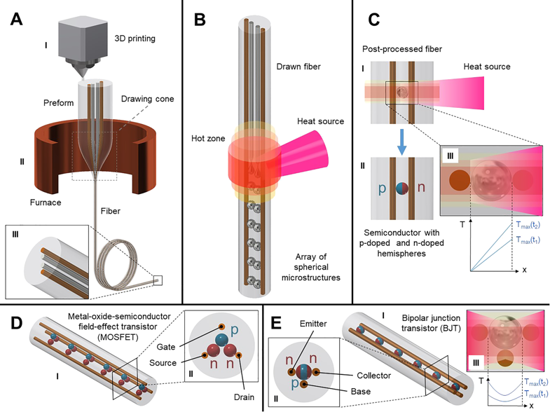
VLSI-Fi: Conceptual schematics of the VLSI-Fi technique representing the “2D + 1D + 0D” approach. a The 3D-printed preform a (I) is thermally drawn a (II) into a long, thin fiber that preserves the cross-sectional geometry of the preform (2D). b Axial patterning of the fiber via spatially coherent, material-selective capillary breakup (+1D), resulting in the assembly of initially continuous, separate cores into arrays of discrete devices contacted in parallel. c Segregation-driven control of doping in post-breakup semiconducting particles, allowing control of an individual device’s internal architecture c (II) via thermal gradient c (III). d (I) Schematic illustration of Metal-oxide-semiconductor field-effect transistor (MOSFET) through VLSI-Fi, where the p-type and n-type semiconductors are shown in blue and red, respectively. The golden continuous rods embedded in a silica fiber act as gate, source, and drain. The resulting fiber cross section is shown in d (II). Similarly, e (I) shows a schematic picture of a bipolar junction transistor (BJT) realized by VLSI-Fi, achieved with impinging heat sources from both the emitter and collector sides. The fiber cross section e (II) shows the emitter, collector, and base of the BJT (continuous rods embedded in the fiber), with the p-type and n-type semiconductors of the n-p-n junction shown in blue and red, respectively
A preform is built, and while there are several ways to do so, 3D printing is one possible technology. Fibers can also be woven into different structures for added strength and used as synthesis platforms for the production of materials, as well as sensors. The benefits of 3D printing can be enjoyed too, made easily accessible, affordable, and user-friendly in many cases. The authors state that 3D printing is also attractive for fabrication due to feasibility with so many different types of materials, to include thermoplastics, biomaterials, and more.
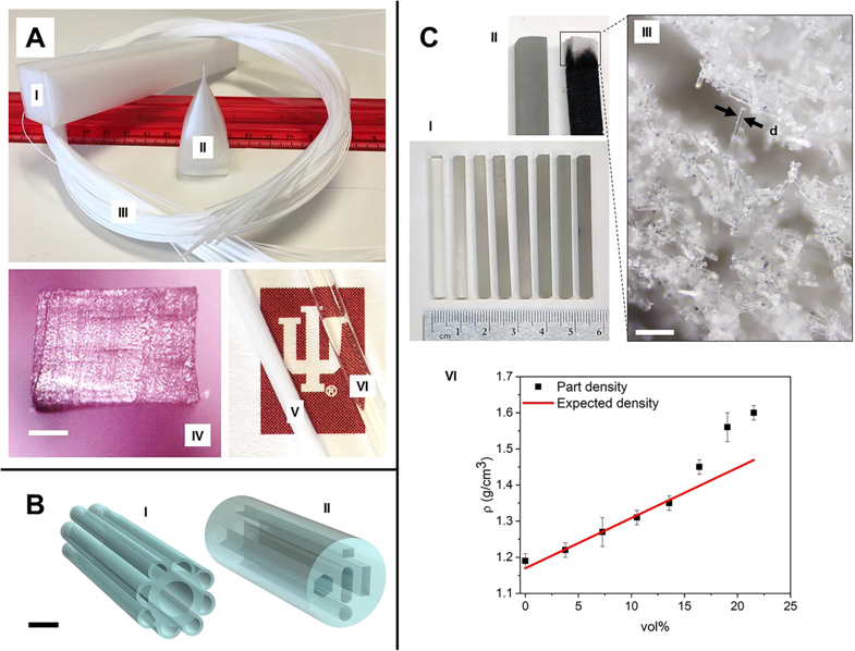
3D printed preforms: a (I) Square-base 3D printed polycarbonate preform. a (II) Drawing cone. a (III) Resulting polycarbonate fiber after thermal draw. a (IV) Fiber cross section after the draw process, with no layer delamination. The cross section is rectangular due to non-isotropic porosity of the infill pattern (scale bar 200 μm). a (V) Drawn fiber before annealing. a (VI) Drawn fiber after annealing with apparent optical transparency. b CAD models of Glass preforms, successfully realized in soda-lime glass with high-precision extrusion-based 3D printing. b (I) Structure mimics blue tarantula hair. b (II) Preform model with non-equilibrium cross-sectional geometry (scale bar 1 cm). c (I) Square-shaped glass samples with increasing glass infill (from left to right), printed with SLA technique. c (II) Detail of glass sample before baking (left) and during baking (right). In the latter, it is possible to see the black coloration resulting from the carbonized residues of resin, while the tip presents white coloration after these residues are ashed out. c (III) Picture under microscope of the ashed-out section (scale bar 200 μm), where the white coloration is a result of the natural color of the compacted milled fibers in an interconnected porous structure. Moreover, the nominal width of the glass fiber, indicated in the image by d, correlates to the expected values of 16 μm (#38 Fiber Glast). c (IV) A plot of the printed glass preforms densities (ρ) as function of the volume fraction of glass fibers mixed with resin, along with the average density of the print material
In using the concept of very large-scale integration (VLSI) for fibers (VLSI-Fi), the researchers can combine liquid phase processing techniques to create a ‘toolbox’ for fabricating a range of devices and systems. Here, the team focuses on ‘narrower aspects’ of VLSI-Fi and the following:
- Preform 3D printing
- In-fiber circuit assembly
- Segregation-driven doping control
“In addition, the FAMES Lab has the ability to process high-temperature materials, alongside the more traditional use of thermoplastics in additive manufacturing, allowing us to take advantage of properties such as the high electron mobility in Si/Ge, as well as the future use of lead zirconate titanate (PZT)/BaTiO3 composites for piezoelectric applications having large piezoelectric coefficients compared to polymers and higher acoustic bandwidth,” stated the researchers.
Fibers are often used in the biomedical realm, for applications related to medical, physical, and chemical sensors that could monitor stress, temperature, moisture, and other settings.
“Examples of smart fiber development include a neural fiber probe composed of a polymer and metal core composition that enables flexibility and bending stiffness of the neural probe as it provides in vivo optogenetic stimulation and delivers drugs as an input in order to record feedback electrical and physiological output signals,” state the researchers.
“Another example is a fiber integrating microfluidic principles with complex cross-sectional geometries and meter-long microchannels which analyzes cell separation by dielectrophoresis (DEP). Live and dead cells are separated by inertial and dielectrophoretic forces by sheathless, high-throughput microfluidic cell separator which contains conductive materials in the microchannels.”
Biosensors can also be created in a multitude of different ways and can monitor cells, bacteria, DNA, and more. Ultimately, the researchers see VLSI-Fi as allowing for the realization of product in numerous areas of technology, beginning with active biomimetic scaffolds.
“We believe that this method will deliver a new class of durable, low cost, pervasive fiber devices, and sensors, enabling integration of fabrics met with human-made objects, such as furniture and apparel, into the Internet of Things (IoT). Furthermore, it will boost innovation in 3D printing, extending the digital manufacturing approach into the nanoelectronics realm,” conclude the authors.
3D printing has opened up a wide expanse of materials science, to include innovation with fibers and sensors for wearables, fiber optics, and biomedical applications. What do you think of this news? Let us know your thoughts! Join the discussion of this and other 3D printing topics at 3DPrintBoard.com.
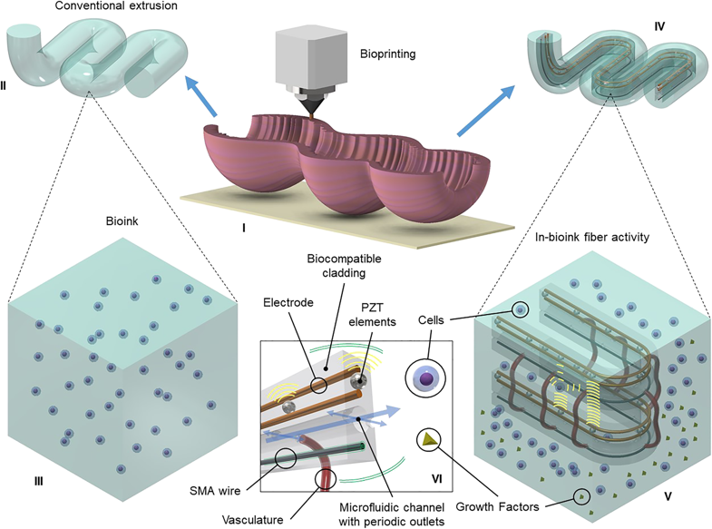
Biological interfacing. (I) Three-dimensional bioprinting of a tissue. (II) Standard microextrusion of bioink. (III) Conventional bioink with cells suspended in hydrogel. (IV) Novel coaxial microextrusion of biointerfacing fiber coated in bioink. (V) Close-up view of fiber where biointerfacing occurs: epithelial cells and vascular epithelial growth factors are excreted from different microchannels and result in cellular self-assembled vasculature between two orifices; piezoelectric elements measure surrounding cell density by ultrasound; and shape memory alloy wires provide peristaltic motion in the tissue. (VI) Visualization of biointerfacing fiber and its components
Subscribe to Our Email Newsletter
Stay up-to-date on all the latest news from the 3D printing industry and receive information and offers from third party vendors.
Print Services
Upload your 3D Models and get them printed quickly and efficiently.


You May Also Like
ROBOZE Buys Dimanex Assets to Build “Physical AI” Platform
Dutch firm Dimanex got its start as an MRO platform for the railways. The company had a contract with the Dutch Army in 2018, and later that year signed one...
3D Printing Financials: Nano Dimension Reports Q1 Growth Amid Restructuring and Asset Sales
Nano Dimension (Nasdaq: NNDM) started 2026 with a much larger first quarter business than it had a year ago, mainly because Markforged is now part of the company and included...
DMG Mori Joins $10M Defense 3D Printing Program
To look at the Biden administration and the Trump administration that succeeded it and find areas of policy overlap is obviously a bit of a challenge. But such areas certainly...
3D Printing & Drone Dominance: Speed, Performance, and Derisking the Supply Chain
A shift is underway in drone manufacturing. Government programs like the U.S. Department of War’s Drone Dominance, a $1.1 billion effort to deliver low-cost, one-way attack (OWA) sUAS at scale,...