
Nanoshaping — It’s Additive Manufacturing, But With Tiny Forces And Not Materials

It’s an entirely new method of “additive manufacturing” where the only thing added is 1 or 2 gigapascals of force. In case you’re wondering, one square inch of water results in 0.0361396333 pounds per square inch – and that’s 0.000000249 gigapascals.
It might better be called 3D stamping, but by using “laser shock imprinting,” the process creates 3D crystalline metallic structures as small as 10 nm with ultrasmooth surfaces – and it does so at room temperature.
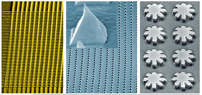 The method creates large-area patterns of three-dimensional nanoshapes from metal sheets and could lead to inexpensive, mass produced innovations such as “plasmonic metamaterials” for use in advanced technologies. Plasmonic metamaterials are custom made composites (combinations of metallic and dielectric materials designed to achieve optical properties not seen in nature), and their properties stem from the unique structure of such composites which include features smaller than the wavelength of light separated by subwavelength distances.
In a paper on the subject, “Large Scale Nanoshaping of Ultrasmooth 3D Crystalline Metallic Structures,” authors Huang Gao, Yaowu Hu, Yi Xuan, Ji Li, Yingling Yang, Ramses V. Martinez, Chunyu Li, Jian Luo, Minghao Qi, and Gary J. Cheng say the benchtop method enables thin layers of metal to be shaped with nanoscale precision. The authors are comprised of doctoral students and professors from Purdue, a researcher from Harvard and Madrid Institute for Advanced Studies, and a professor from the University of California, San Diego.
The technique results in uniform nanopatterns from metamaterials and have engineered surfaces with features, patterns or elements which provide unprecedented control of light. The researchers say the technique could result in innovations like high-speed electronics, advanced  sensors, and solar cells. The process creates crystalline forms from metals which potentially give them “ideal mechanical and optical properties.”
Shapes like nanopyramids, gears, bars, grooves, and a fishnet pattern are thousands of times thinner than the width of a human hair, and the researchers have used the technique to stamp nanoshapes from titanium, aluminum, copper, gold, and silver. This “shock-induced forming” method sharply defines corners and vertical features.
“These nanoshapes also have extremely smooth surfaces, which is potentially very advantageous for commercial applications. Traditionally it has been really difficult to deform a crystalline material into a nanomold much smaller than the grain size of starting materials, and due to the size effects the materials are super-strong when grain size has to be reduced to very small sizes,” Cheng says. “It is very challenging to generate metal flow into nanomolds with high-fidelity 3D shaping.”
Cheng adds that the work has also resulted in hybrid structures which combine metal with graphene, and that these hybrid materials enhance the plasmonic effect and bring “metamaterial perfect absorbers,” or MPAs.
The technique uses a pulsed laser to generate “high strain rate” imprinting of metals into the nanomold.
“We start with a metal thin film, and we can deform it into 3D nanoshapes patterned over large areas. What is more interesting is that the resulting 3D nanostructures are still crystalline after the imprinting process, which provides good electromagnetic and optical properties,” said Cheng.
The project was supported by the National Science Foundation, National Institutes of Health, Defense Threat Reduction Agency, Office of Naval Research, and the National Research Council.
How do you define what is, and what isn’t, additive manufacturing? Please feel free to include your definition at the Nanoshaping forum thread at 3DPB.com.
Subscribe to Our Email Newsletter
Stay up-to-date on all the latest news from the 3D printing industry and receive information and offers from third party vendors.
Print Services
Upload your 3D Models and get them printed quickly and efficiently.


You May Also Like
Mikhail Gladkikh on Digital Inventory: “Think of It as Netflix for Manufacturing”
As manufacturers continue looking for ways to reduce supply chain risk, additive manufacturing (AM) is increasingly being discussed as more than just a production tool. Across aerospace, energy, defense, and...
ROBOZE Buys Dimanex Assets to Build “Physical AI” Platform
Dutch firm Dimanex got its start as an MRO platform for the railways. The company had a contract with the Dutch Army in 2018, and later that year signed one...
MORSAN and LEHVOSS Work on 3D Printing for Food and Beverage
For many years, LEHVOSS has made specialized 3D printing materials such as high-temperature polyamide and high-flow PEEK. Now it has teamed up with MORSAN to develop a 3D printing offering...
3D Printing & Drone Dominance: Speed, Performance, and Derisking the Supply Chain
A shift is underway in drone manufacturing. Government programs like the U.S. Department of War’s Drone Dominance, a $1.1 billion effort to deliver low-cost, one-way attack (OWA) sUAS at scale,...