
Mass 3D Printing for Microchip Packaging Enabled with New Optomec Software


Embedding electronics and sensors inside 3D printed objects in a single build process has been a sought-after goal for the sector for some time. Not only does this innovation make it easier to print more advanced components, but it could revolutionize industries like consumer goods, autonomous vehicles, defense, and healthcare. At the helm of this revolution are companies like Optomec, stirring an industry that relies on complex supply chains and long development times that cause electronic components to become obsolete.
Thirty years after its inception, this New Mexico-based company is ready to take 3D printed electronics to the next level. As a manufacturer of some of the most sophisticated electronics 3D printers, Optomec just announced the release of a new production control software explicitly designed for high-volume manufacturing of printed electronics.
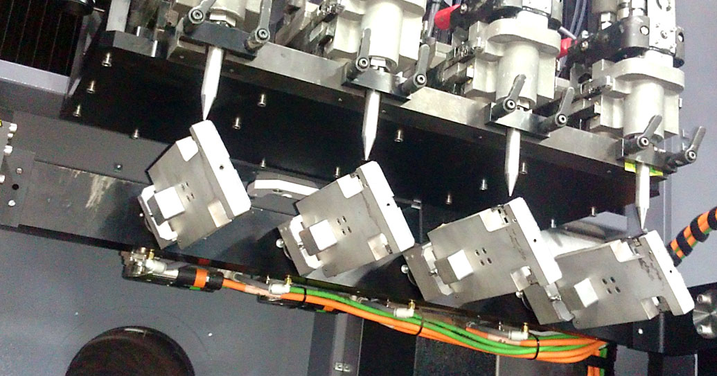 Lite On’s production set up for 3D printing antenna on phones, like iPhones. Image courtesy of Optomec.
Specifically created for Optomec’s high-volume production customers with applications such as multi-chip packaging, millimeter-wave integrated circuits, heterogeneous chip integration, and 3D printed antennas for 5G devices, the proprietary software called KEWB “simplifies everything,” says Optomec. During its development, the team drew inspiration from the field experience of Optomec’s 400 installed base of Aerosol Jet industrial printers, which precisely and accurately deposit electronic inks onto substrates.
Multiple companies offer methods for 3D printing conductive materials, mainly silver inks. Still, Optomec’s Aerosol Jet systems are already used by major smartphone manufacturers to 3D print conductive traces onto parts, explained 3DPrint.com’s Editor in Chief Michael Molitch-Hou in a Forbes.com article.
By jetting extremely fine droplets of nanoparticle conductive inks onto circuit boards and components, Aerosol Jet technology can produce conductive features as fine as ten microns in width. Techniques like aerosol jetting have emerged as the holy grail of 3D printed electronics. By applying electronic inks to a substrate, manufacturers can quickly make devices and components that are ever more complex.
Optomec’s new Aerosol Jet HD2 printer with ultra-high printing resolution and integrated vision-based alignment has been optimized to support millimeter-wave integrated circuit printing for complete production applications that have been proven to improve overall device efficiency and performance, explained Optomec.
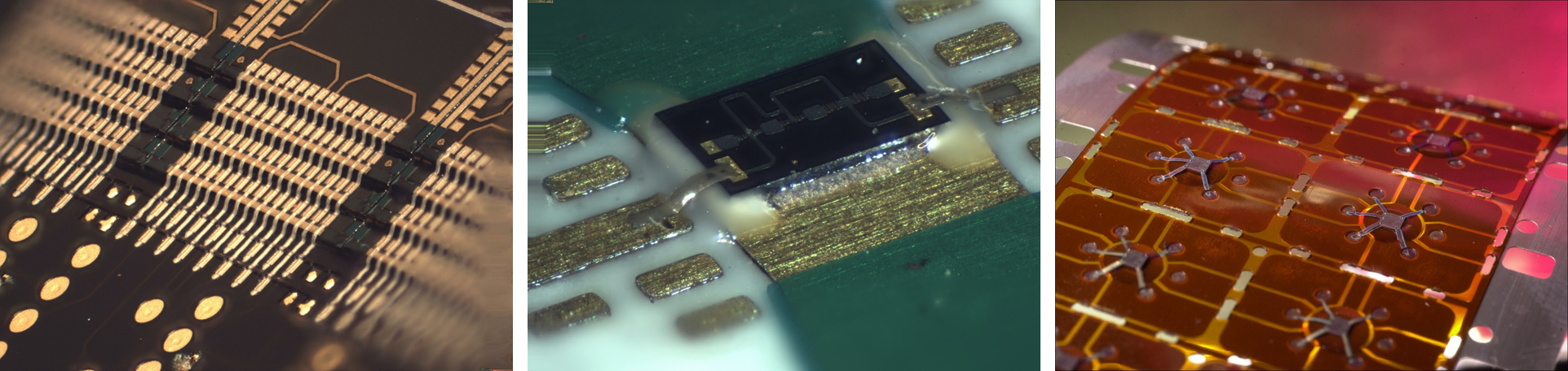 Semiconductor Packaging examples showing Printed 3D Interconnects for 3D stacked die (l), mmWave (c), and flex circuit (r). Image courtesy of Optomec.
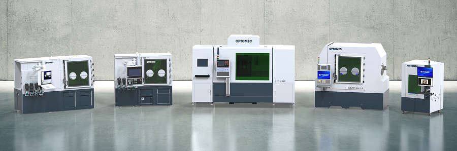
Optomec’s suit of printed electronics machines, from its patented Aerosol Jet systems to its LENS and Huffman 3D printers for metal component production and repair, enable manufacturers to create extremely fine 3D electronic structures – such as circuits, sensors, antennas, and interconnects – with features as small as ten microns using nanoparticle inks.
Together, these unique printing solutions work with the broadest spectrum of functional materials, ranging from electronic inks to structural metals and even biological matter. As a result, the machines are widely used in the aerospace and defense, energy, medical device, advanced electronics packaging, and research segments. The brand has delivered more than 600 of its proprietary additive manufacturing systems to more than 250 customers around the world, including countless blue-chip manufacturing companies, such as GE, Samsung, Raytheon, Siemens, Lockheed Martin, and LiteOn, as well as government agencies like the US Air Force, US Navy, US Army, and NASA, and renowned brands like Rolls Royce and Xerox.
 Optomec LENS and Aerosol Jet Printers. Image courtesy of Optomec
The release of the KEWB software follows the recent introduction of the brand’s proprietary Aerosol Jet HD2 printer, a precisely printed electronics and material dispense platform that combines high-speed, sub-micron resolution, SEMI-compliant inline conveying, and advanced alignment optics over a 300 x 300 mm work area.
Commenting on the new KEWB software, Optomec Software Development Manager Dave Gleason said, “it’s configurable for multiple user levels, so the engineer sees a full vision tool kit while the machine operator sees a simplified, pictorial sequence of process steps. The entire software approach is focused on production.”
3D printing in electronics can be highly beneficial and ideal for complex electronics. Moreover, as Optomec has proven, its technology is advantageous not only for prototyping but for full-scale manufacturing. This opens the door for additive manufacturing to benefit in the future in areas where it previously could not.
Subscribe to Our Email Newsletter
Stay up-to-date on all the latest news from the 3D printing industry and receive information and offers from third party vendors.
Print Services
Upload your 3D Models and get them printed quickly and efficiently.


You May Also Like
3D Printing News Briefs, July 1, 2026: Prosthetics, Drug Delivery, & More
We’re focused on healthcare and research in today’s 3D Printing News Briefs, including 3D printed prosthetics, patient-specific implants, drug delivery, and more. Read on for all the details! Students from...
3D Printing News Briefs, June 18, 2026: Reseller, Relocation, Metal Space Powder, & More
We’ll start with business news in today’s 3D Printing News Briefs, as XJet appointed a value-added reseller in Germany, BIO INX is expanding its presence in the Italian market, and...
CEO Yoav Zeif on Why Stratasys’ Markforged Acquisition Is Really a Bet on Industrialization
When Stratasys announced plans to acquire Markforged, the immediate focus was on the deal. Markforged is one of the most recognizable names in additive manufacturing (AM), known for its continuous...
Stratasys Acquires Markforged, Analysis of AM’s Latest Consolidation Move
A very long time ago, in 2023, the additive manufacturing (AM) industry was enraptured over the attempts by a large chunk of its publicly traded original equipment manufacturers (OEMs) to...