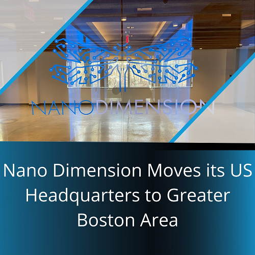
Nano Dimension’s Electronics 3D Printing HQ in US Moves to Massachusetts


Recently, I had the opportunity to visit the Israeli headquarters of printed circuit board (PCB) leader Nano Dimension (Nasdaq: NNDM), which specializes in Additively Manufactured Electronics (AME), micro additive manufacturing, Printed Electronics (PE), and High-Performance Electronic Devices (Hi-PEDs). The company has now announced the opening of its new US headquarters in Waltham, Massachusetts, located in the Boston metropolitan area. This relocation to an area much closer to several strategic R&D institutions is part of Nano Dimension’s business plan.
“We are excited to strengthen our presence in the nation’s academic research and technological innovation center. Our multi-year growth initiative is dependent on being near the institutions and consortia that are already – or will soon become – our customers,” explained Nano Dimension’s Chief Revenue Officer Sean Patterson, the President of Nano Dimension USA.
As Hanan Gino, CPO and Head of Strategic M&A at Nano Dimension, told me, the company wants to “revolutionize the electronics industry.” The best way to do this is by partnering with and acquiring companies that can help it reach this goal. Nano Dimension is working off a technology roadmap that will progress a new production model for 3D printed electronic (and other) devices through advanced materials, 3D printing, deep learning AI, and integrated surface mount technology (SMT). The production model will allow for self-improving, intelligent automation and processes that are more environmentally friendly and secure.
Nano Dimension looks for companies in materials development, equipment vendors in its chosen sector, and, as Gino said, “companies who will give us the presence in the right market,” as well as those with complementary technology to its own AME solution. With its US headquarters relocating to the Boston area, the company is well-positioned near academic and research institutions, like Harvard, MIT, and Boston University, that have already adopted its AME, Micro-AM, and PE solutions. The new facility is also near several R&D labs and more public and private universities as well, which means Nano Dimension is also close to an extremely high-tech talent pool.
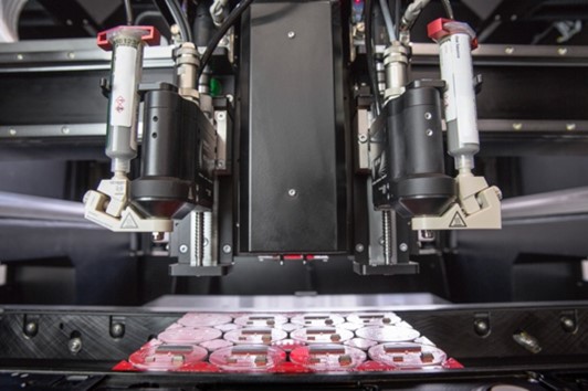
3D printing electronics. Image courtesy of Nano Dimension.
“Even beyond the four strategic acquisitions completed in the past year, we are expecting tremendous growth in our customer base and our staff moving forward. It is important for us to take part in the Massachusetts area’s thriving professional and research ecosystem,” Patterson said.
Nano Dimension’s new headquarters will feature customer support and fabrication facilities, which can be used to support its AME Academy events and other local organizations. The facility will also house increased sales operations. To help lead the way in its new home, Nano Dimension has welcomed PCB marketplace veteran Gene Howard Weiner, through his Massachusetts firm Weiner International Associates, as a consultant. Additionally, the new AME Standards Manager in the company’s US home is Dana Korf, Principal Consultant at Korf Consultancy.
Patterson said, “These are two figures of immense technical knowledge and vast experience within the business of software, OEMs, and electronics manufacturing. Their professional networks will allow us to take full advantage of emerging opportunities.”
Nano Dimension will keep its marketing, sales support, NaNoS printing services and logistics center open in Sunrise, Florida. The company plans to host an official open house for its new Massachusetts office later this summer, though current and prospective customers can come visit by appointment.
Subscribe to Our Email Newsletter
Stay up-to-date on all the latest news from the 3D printing industry and receive information and offers from third party vendors.
Print Services
Upload your 3D Models and get them printed quickly and efficiently.









You May Also Like
Axtra3D Rolls Out New Software, Wash and Cure Systems at Formnext 2026
Axtra3D has made a number of strides forward of late, introducing new software workflow tools, a new FR material together with Arkema, and new washing and curing stations. The company...
3D Printing News Briefs, November 14, 2026: Chuck Hull, Tungsten Carbide, Movie Costume, & More
In this weekend’s 3D Printing News Briefs, we are of course starting off with some Formnext news ahead of the big event this coming week. Then we’ll move on to...
Two Farsoon Machine Launches & How Chinese AM OEMs Are Shifting Focus
In posts last month about Eplus3D and how it’s scaling production for the AI infrastructure market, I focused on how the Chinese additive manufacturing (AM) landscape looks poised to intensify...
3D Printing News Briefs, November 11, 2026: Financing, Distributor, Kickstarter, & More
We’re starting off with exciting AMUG news in today’s 3D Printing News Briefs, as Neil Hopkinson was selected for the 2027 Innovators Award. Then we’ll move on to business, with...