Microwave Electronic Circuits Made via Low-Cost 3D Printer & Plastic Filament
In the electronics industry, 3D printing has been used to fabricate sensors, stretchable electronics, and conformal electronics, and to make waveguide devices and antennas for microwave devices. That’s because the technology can be used to design dielectric substrates for specific applications and multilayer devices with several dielectric layers, working with a wide variety of materials at different densities.
Pushing the envelope further is a team of researchers from Miguel Hernández University of Elche in Spain, which published a study, “Low-Cost Additive Manufacturing Techniques Applied to the Design of Planar Microwave Circuits by Fused Deposition Modeling.” The paper details their work using an inexpensive FDM 3D printer and plastic-based filaments to manufacture and implement microwave electronic circuits.
“Since all commercial filaments available for this type of 3D printer are not intended to implement microwave devices, it is necessary to obtain the electrical parameters of each material (dielectric constant and loss tangent). Additionally, since FDM does not allow the printing of metallic materials and the conductive filaments currently available do not have high conductivity, for microwave circuits it is necessary to develop a technique for the metallization of 3D printing parts, using copper plates attached directly to the substrate, as it is done with conventional high-frequency substrates,” the researchers wrote. “Additionally, due to the fabrication process of the circuit, which comprises, on the one hand, the fabrication of a substrate based on a plastic pseudo-thermofused layered structure, and for the other, the use of epoxy adhesives to glue the copper boards, it is necessary to check if the whole process results in a reliable structure.”
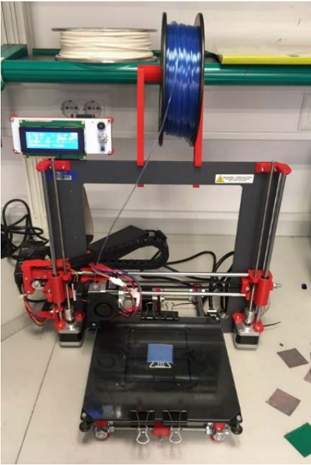
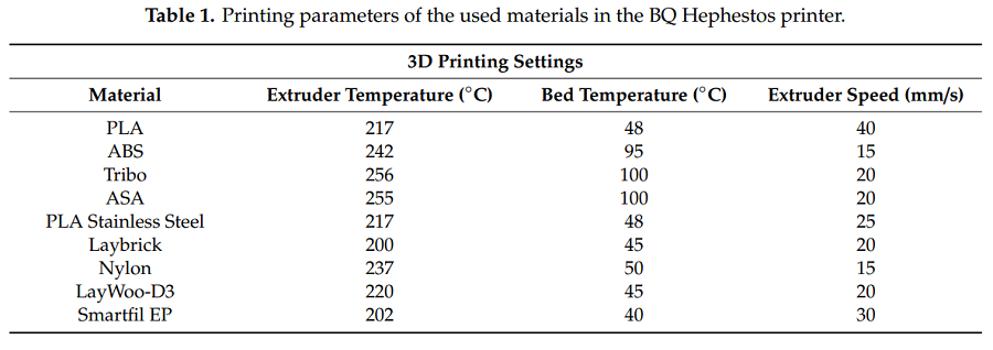
The team chose a low-cost Prusa i3 Hephestos 3D printer for this study, which uses extrusion-based fused deposition modeling (FDM) technology. Cura software was utilized to adjust the various 3D printing parameters, below, for all of the materials used.
The researchers analyzed many standard 1.75 mm diameter filaments to “obtain different electrical properties for the design of microwave circuits,” and chose these to use in the study:
- PLA from German RepRap: polymer made of lactic acid molecules
- ABS from Fillamentum: amorphous, impact-resistant thermoplastic
- Iglidur I180-PF (Tribo) from Igus: friction-resistant, good response to wear degradation
- ASA from Fillamentum: UV- and water-resistant thermoplastic
- PLA Stainless Steel from Protopasta: made of PLA and grinded filament from pulverized stainless steel
- Laybrick filament from CC-PRODUCTS: made of sandstone, offers a similar surface finish to ceramic or stone
- Nylon 230 filament from Taulman: synthetic polyamide
- LayWoo-D3 filament from CC-PRODUCTS: made of wood fibers and PLA, offers a similar surface finish to wood
- Smartfil EP filament from Fillamentum: made of PLA and Calcium carbonate, offers a similar surface finish to limestone
As you can see below, the sheets forming the 3D printed microwave circuit substrates can be classified as either an outer layer or an inner layer. Because the mechanical stiffness of the substrate can be affected by how thick the outer layers are, the team states that they “should be solid with a filling pattern density percentage of 100%,” and fabricated in a rectilinear pattern in order to decrease surface roughness and avoid porosity. However, it doesn’t matter which fill density or pattern is used for the inner layers.
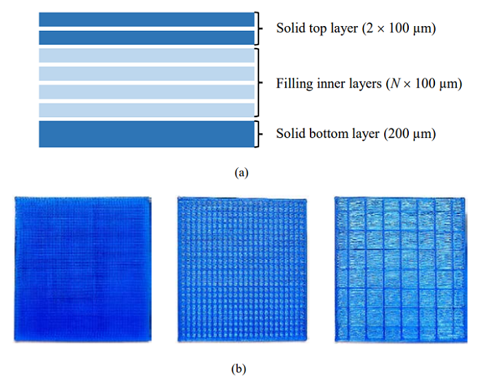
(a) Structure of the printed layers of the substrates. (b) Linear printing pattern of 3D material with different filling densities, 100%, 50% and 15%.
The 3D printed substrate was metallized by attaching two hydraulically pressed 35 µm copper sheets, using nonconductive 2216 B/A epoxy glue GRAY, to each side. The researchers built the microwave circuits with a Protomat S42 from LPKF numerical control milling machine, and once the glue has solidified the copper to the substrate, it can be used.
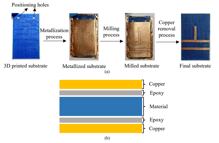
(a) Printed circuit board manufacturing process. (b) Printed circuit structure of the different materials.
Any fabrication errors, like bubbles and voids in between layers, a lack of homogeneity in the layers, or too much adhesive, could result in potential failure of the 3D printed circuit’s structural integrity and performance. So, in order to “verify the correct metallization and fabrication of the substrate,” the team used fast and accurate but inexpensive ultrasonic nondestructive techniques to conduct a structural analysis, and turned to time and frequency domain analysis techniques of circuit C-scans to see if there were any structural issues or defects.
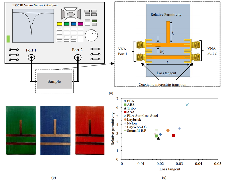
(a) Setup for the dielectric permittivity and loss tangent measurements. (b) Resonator and transmission line on different materials: ABS, PLA, and ASA. (c) Electrical characteristics calculated for different substrates.
Additionally, the researchers characterized each filament’s electrical properties in the microwave frequency range, and implemented both standard and novel microwave filters in microstrip and stripline technology.

(a) Resonator and transmission line for PLA with 70%, 50% and 15% densities. (b) Electrical characteristics for different filling densities of the PLA substrate.
Finally, the team designed and fabricated simple planar microwave circuits in a proof of concept to demonstrate how feasible it is to use 3D printing for this application.
“The designed devices were manufactured and measured with good results, which demonstrates the possibility of using low-cost 3D printers in the design process of planar microwave circuits,” they wrote.

Left to right, top to bottom: successive layers inside the circuit in steps of 150 µm approximately.
By following this team’s methodology, other researchers could learn to add more complex microwave circuit structures to their work, including designing waveguide filters “by means of periodic structures where the additive techniques allow the design of the waveguide sections to obtain a higher rejection bandwidth,” and where correctly configuring the 3D printer enables the design of a “coupling factor of the different filter sections.”
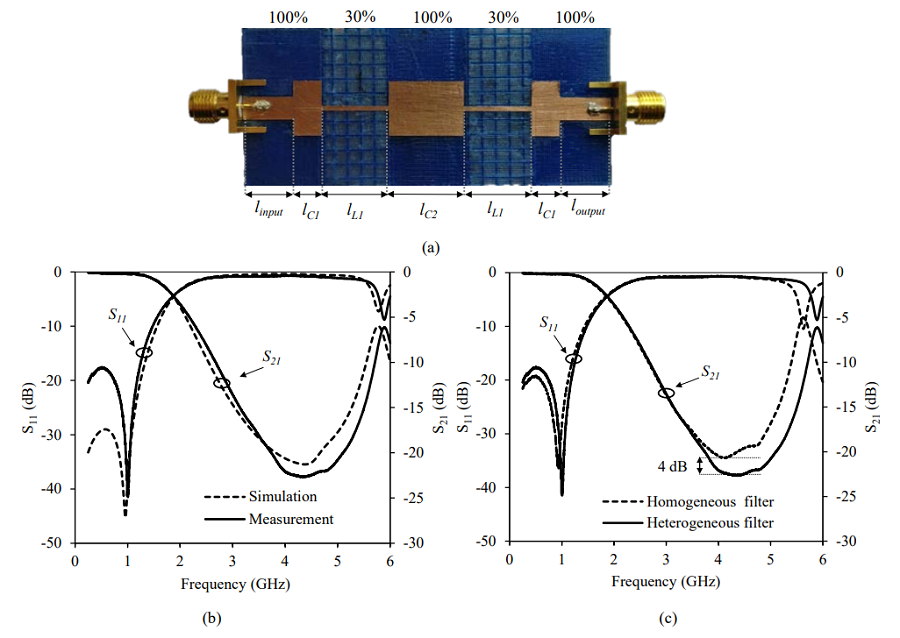
(a) Stepped impedance filter manufactured with 100% density. (b) Measured and simulated response of the stepped impedance filter with a 100% density substrate.
“The ultrasonic structural analysis has shown the reliability of the manufacturing process. Finally, to check the different possibilities offered by the additive manufacturing process presented, different simple and complex stepped impedance filters were implemented in microstrip and stripline technology. Good results were obtained in both technologies, with better performances when additive possibilities, such as different substrate densities are used, so it can be concluded that additive manufacturing techniques offer wide possibilities in the design of planar microwave circuits,” the researchers concluded.
Subscribe to Our Email Newsletter
Stay up-to-date on all the latest news from the 3D printing industry and receive information and offers from third party vendors.
Print Services
Upload your 3D Models and get them printed quickly and efficiently.
You May Also Like
Holcim, COBOD and PERI Print 12 Unit Social Housing Project in France
Holcim has announced that a 12-unit residential structure, ViliaSprint² in Bezannes, France, was finished in a year. Nice to see that people seem to be properly building structures rather than...
Former Spy/Congressman to Head New Federal Division at Construction 3D Printing Powerhouse ICON
Earlier this year, the Department of Defense (DOD) broke ground on its biggest additive construction (AC) project to date, aiming to complete ten new barracks at Texas’s Fort Bliss US...
U.S. Army Begins Construction of 10 3D Printed Barracks at Fort Bliss
The U.S. Army has begun construction of 10 3D printed barracks at Fort Bliss in El Paso, Texas, in what is being described as the Department of Defense’s largest 3D...
PALFINGER and ICON Partner to Push 3D Printed Construction Into Heavy Industry
Construction 3D printing pioneer ICON is teaming up with Austrian crane specialist PALFINGER in a move that could help bring large-scale 3D printing closer to mainstream construction use. The two...


