
Nanyang Technological University: Inkjet Printing of ZnO Micro-Sized Thin Films

![]() In ‘Inkjet-printed ZnO thin film semiconductor for additive manufacturing of electronic devices,’ thesis student Van Thai Tran, from Nanyang Technological University, delves into the realm of fabricating products with conductive materials. As inkjet printing continues to gain popularity for researchers and manufacturers, it is the vehicle for creating a wide variety of innovations, to include tissue engineering and more. Here, however, Tran develops and examines ZnO thin film to promote electrical qualities in hopes of expanding 3D printing processes further overall.
In ‘Inkjet-printed ZnO thin film semiconductor for additive manufacturing of electronic devices,’ thesis student Van Thai Tran, from Nanyang Technological University, delves into the realm of fabricating products with conductive materials. As inkjet printing continues to gain popularity for researchers and manufacturers, it is the vehicle for creating a wide variety of innovations, to include tissue engineering and more. Here, however, Tran develops and examines ZnO thin film to promote electrical qualities in hopes of expanding 3D printing processes further overall.
The author understands the many benefits of 3D printing, as they have unfolded since the mid-80s. Today, the technology has progressed far beyond rapid prototyping, and a wide range of functional products are being made.
“It is expected that 3D printing will play a significant role in the fabrication of goods soon. As a result, the demand for printed functional devices has been raised to fulfill the need for printed consumable products, which are composed of multi-materials,” states Tran. “Hereby, the printed functional devices are not only basic electrical elements, such as resistors, capacitors, and transistors, but also advanced electric devices, such as sensor, solar cells and batteries.
“The construction of a product using 3D printing requires a combination of structural material and functional material. To accomplish the fully additive manufacturing process, printing of functional materials, such as conductor and semiconductor, is crucial.”
ZnO is helpful today in applications like:
- Optoelectronics
- Electronics
- Sensors
- Piezoelectric devices
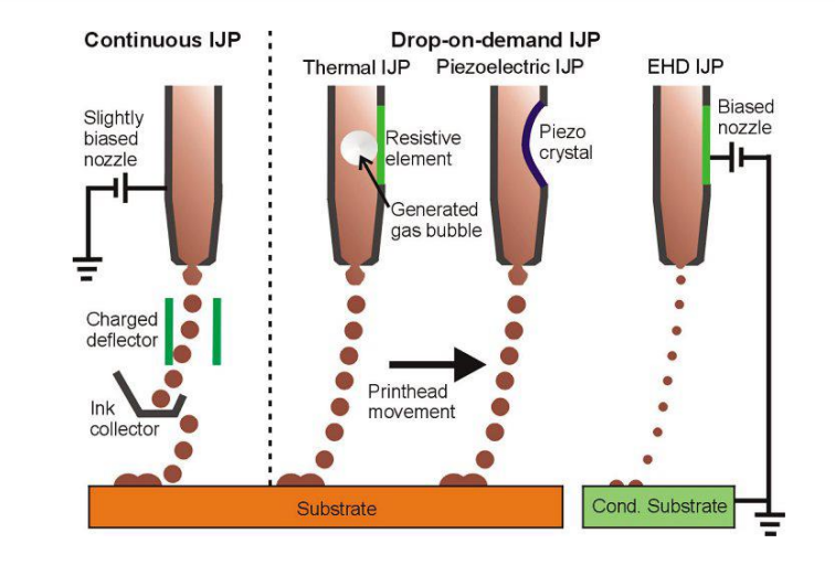
Inkjet printing technologies: Continuous inkjet printing and Drop-on-demand Inkjet printing and electrohydrodynamic inkjet printing
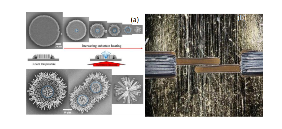
Tran does raise concerns, however, regarding the use of ZnO in inkjet printing—such as the likelihood that it may cause band bending, resulting in defects in the 3D printed products. Band bending issues must be controlled and ‘engineered’ to create a device that is highly functional, lending central focus to this study, along with creating a successful way to improve on using the photolithography process, and investigating issues in annealing.
As an intrinsic n-type semiconductor, ZnO also possesses piezoelectric properties, capable of generating voltage under pressure—and causing it to be suitable for applications requiring sensors and actuators. As for thin film transistors, ZnO is an attractive option due to compatibilities with LCD applications and a variety of miniaturized electronics. As Tran mentions, ZnO is also especially suited to UV photodetector applications too.
In this project, Tran fabricated thin films via inket printing, but modifications were made with annealing—decreasing the band bending. The author also discovered that electrical properties were greatly improved due to heat treatment, with film conductivity impacted by band bending changes.
“The successful inkjet printing of micro-sized ZnO thin films and the integrated photodetector has demonstrated the feasibility and great potentials of fabricating sophisticated semiconductor devices using additive manufacturing technology,” concluded the author.
3D printing and electronics have been coupled together since the beginning, allowing for expansive innovations—and allowing many manufacturers to create items never possible. They are also able to enjoy much greater sustainability in production, whether in creating breakthrough techniques in manufacturing, liquid materials for electronic applications, or wearables. Find out more about semiconductors in AM manufacturing here.
Discuss this article and other 3D printing topics at 3DPrintBoard.com.
Additively fabricated ZnO nanostructures. (a) Selectively grown ZnO nanowire from inkjet-printed pattern (b) Electro-spinning ZnO nanowire

Printer structure and printing process to prepare the thin film. (a) Printer structure shows the main components and three-axes of the printer. (b) Optical photo of the printer. (c) Optical picture of the cartridge, including ink container and nozzles. (d) The schematic of the droplet watcher, which is the system to observe the generation of droplet before running the printing
Subscribe to Our Email Newsletter
Stay up-to-date on all the latest news from the 3D printing industry and receive information and offers from third party vendors.
Print Services
Upload your 3D Models and get them printed quickly and efficiently.


You May Also Like
3D Printing News Briefs, April 8, 2026: LiDAR Scanning, Vapor Smoothing, FDM Optimization, & More
We’ll kick off today’s 3D Printing News Briefs with some 3D scanning news from Artec 3D, and then move on to new America Makes Project Calls. Then, Raise3D and AMT...
From Print Farm to Toy of the Year: ZB Designs’ Plastic Empire Takes 3D Printed Fidgets Mainstream
Zack and Berkley Bailey, Co-Owners of ZB Designs, started their business with one 3D printer as a side hustle while still in college. On February 13, 2026, in New York...
Printerior Launches Circdal to Build a Sustainable Architectural Ecosystem with 3D Printing
Robotic arm systems gradually gained traction for years in the large-format additive manufacturing (AM) space, before experiencing a legitimate breakout year in 2025. Pellet extrusion has been the clear winner...
3D Printing Startup Born From University of Missouri Accelerator Eyes Over $10M in 2026 Revenue
Who doesn’t love Shark Tank? I’ve actually never seen an episode, but I can at least say that I love the concept. It’s a concept that has broken through the fourth...