Plasmonics: Nanoscribe Photonic Professional GT 3D Printer Allows for Innovative Solutions


 Are you still wrapping your mind around the world of nanotechnology—and wondering why exactly it is that those brilliant minds in research labs around the world aren’t content enough just to engineer things we ordinary people can see? The first part is manageable, but the last part you will need to get used to as scientists operating at the molecular scale are discovering ways to design far too many structures for valuable applications to give up now. And while we’re add it, Nanoscribe is throwing a new term at you with plasmonics. If you are a researcher, you may be well-familiarized with plasmonics, where light is harnessed using custom structures at the nanoscale, generally in metal.
The German manufacturer of 3D printers, as well as offering software and photoresists, is quite comfortable operating in their micro- and nano-worlds, and they cater to a client base busy innovating on that level. Recently offering their first user meeting in the US at Harvard, Nanoscribe is focused on being able to help others not only study nanotechnology, but to do so in high resolution.
As Nanoscribe points out, while plasmonics are often flat molecular surfaces because of electron beam lithography or direct laser writing, their Photonic Professional GT system is more than capable of creating the lithography, as well as fabricating 2.5D polymer nano-/micro-structures in metal.
“The bigger design freedom in this approach allows for interesting new properties and functionalities,” states the Nanoscribe team.
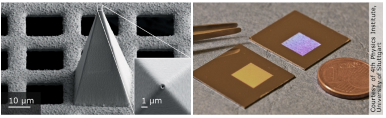
The examples of what can be made with plasmonics are quite impressive, as we get a look into production on the molecular scale, from creating a pyramid with a thin gold film, to an etch mask pattern.
An application note was released recently on the topic as well, where Nanoscribe outlines their 3D printer as that offering the ‘world’s highest resolution.’
“It offers resolution between what can be achieved with electron beam lithography and UV lithography, providing at the same time the full fabrication flexibility for 2D, 2.5D as well as for 3D objects,” states Nanoscribe.
Allowing that the printer can be used in both sterile and non-sterile environments, Nanoscribe developed this hardware for demand research that requires high performance. Maskless lithography can be used on both silicon wafers and glass.
Plasmonic behavior can be achieved through the following:
- Perfect absorber – to 3D print a metamaterial absorber in the MID-IR range, users printed a ‘four-tined fish-spear-like resonator array.’ For thermal conductivity, it was covered in metal film.
- Plasmonic color display – to develop a reflective display ‘based on a surface plasmonic resonance’ for modulating color electronically, users made a 2.5D master pattern array of nanowells. They also offered other processes such as nanoimprinting, the use of aluminum coating and placing of liquid crystals.
- Subwavelength light focusing – users made hollow pyramids coated in gold using a ‘novel methodology’ that used a stronger signal as opposed to subwavelength light focusing.
- Plasmonic nanoantenna – offered as a user-friendly alternative method to make plasmonic nanoantennas—rather than employing electron beam lithography. With the Photonic Professional GT, users were able to pattern polymers and make an etched golden mask.
For those interested in micro-fabrication, it would seem that the Photonic Professional GT is a good place to start if you are heavily involved in research. Tiny parts can be created quickly due to a simple 3D micro printing workflow. According to Nanoscribe, this allows virtual 3D models to be converted into parts for a variety of applications such as:
- Medicine
- Optics
- Fluidics
- Mechanics
Other highlights include:
- Highest resolution commercially available micro 3D printer
- High speed 3D printing by galvo technology
- Accurate and precise by piezo technology
- Two photon polymerization (2PP) of various UV-curable photoresists
- Two-photon lithography of common positive-tone photoresists
- Writing area up to 100 × 100 mm range
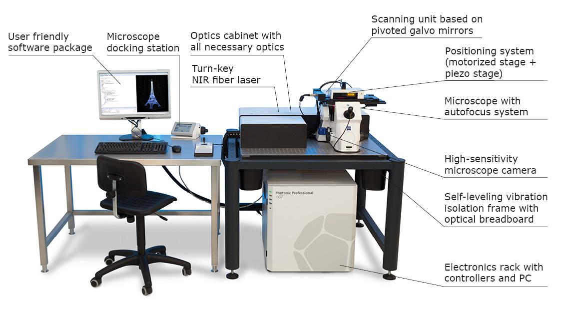
- High-sensitivity microscope camera for realtime observation of the printing process
- User-friendly software package for 3D printing workflow
The goal with this 3D printer was to set new standards for fabrication at this scale not just in 3D printing, but also in maskless lithography, coupling two modes of writing within one machine that offers precise piezo mode for arbitrary 3D trajectories (FBMS) and high-speed galvo mode (MBFS) for speed in the layering method. See Nanoscribe for further information on the Photonic Professional GT. Discuss further in the 3D Printing Plasmonics forum over at 3DPB.com.
Subscribe to Our Email Newsletter
Stay up-to-date on all the latest news from the 3D printing industry and receive information and offers from third party vendors.
Print Services
Upload your 3D Models and get them printed quickly and efficiently.


You May Also Like
3DPOD 302: Digital Inventory for AM with Mikhail Gladkikh, Würth Additive Group
Mikhail Gladkikh has worked in oil and gas for many years. With this background, we obviously talk about energy market turbulence and the adoption of AM in oil and gas....
Spectrum Filaments Gets Investment: How They Could Win in Filament
Spectrum Filaments is a long-time high-quality filament supplier based in Poland. With good tolerances, roundness, and consistency coupled with affordable pricing, the firm has been a mainstay for makers, industrial...
NX Atomics and Sciaky Collaborating to 3D Print Nuclear Components
For decades, the nuclear industry has quietly experimented with and implemented additive. Bouyed by the likes of ORNL, companies such as Westinghouse have 3D printed components serially. We have an...
Incodema3D Buys 14 Metal EOS Systems, Now One of the World’s Largest Metal 3D Printer Operators
Recently, a majority stake of 3D printing service bureau Incodema3D was purchased by AFM Capital. Under new ownership, the Freeville, New York company is now using its cash-rich parent for...