PARC Researchers Move One Step Closer to 3D Printing Electronic Components Within Objects


Tiny Chiplets in Fluid. Photo by: Leah Fasten / Source: MIT Tech Review
3D Printing will heavily be used in the future by individuals wishing to manufacture their own products. Whether it is food, fashion accessories, toys, or even electronics, one day the technology will reach this inevitable point. I have no doubt about it. The question I ponder though is ‘how long will it take us to reach this point?’. Will it be within the next few years, or will it take several more decades? Bill Gates once said, “We always overestimate the change that will occur in the next two years and underestimate the change that will occur in the next ten. Don’t let yourself be lulled into inaction.”
With this in mind, I would be utterly surprised if we don’t find a way to easily 3D print objects with embedded electronics in them by 2024. We have a long way to go though, before we reach this point, however, researchers at PARC in Palo Alto, California have moved us one step closer to reaching this goal.
According to MIT Technology Review, researchers at PARC have come up with a method of placing and printing chiplets onto a plastic substrate in a way that has not been done before.
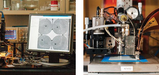
Normally, when electronic devices are made, computer chips are manufactured in bulk on semiconductor wafers. Then they are cut into their own individual units, before being placed on motherboards. The PARC researchers, however, have devised a way to take these semiconductor wafer, chop them up into very small “chiplets”, about the width of a human hair, and then mix them into an ink solution. After complete, these tiny chiplets are provided with positive and negative charges, and then guided to the exact location on a glass substrate, using electrical fields that are generated by wires in a spiral pattern. From there, a specialized roller picks them up and places them on a plastic substrate, where a special type of 3D printer wires them together.
Unless you are an electrical engineer, you are probably rereading the previous paragraph again, trying to understand what it just explained. It’s OK, I don’t entirely understand the whole process either. It’s not the method that is important to most of us, but rather the implications that this method provides for 3D printing.
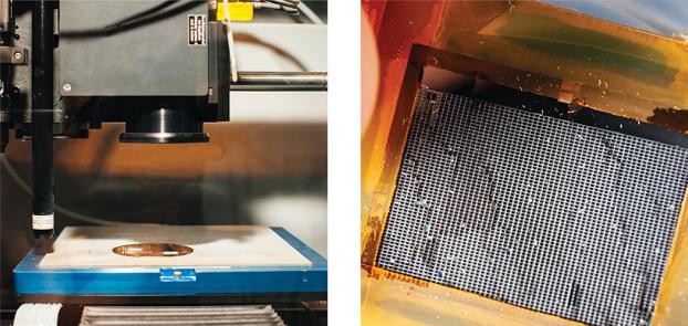
Laser Tools Cuts Wafers Into Chiplets – Photo by: Leah Fasten / Source: MIT Tech Review
Not only does this have the potential of allowing us to create new kinds of computer devices, but it also may have some uses within the 3D printing space.
Because printers can deposit materials on different substrates, this technology could be used to make high-performance flexible electronic devices, tiny sensors festooned with dense arrays of diverse sensors, or 3-D objects with computing functions woven in, says Janos Veres, who manages PARC’s printed-electronics team, explained Janos Veres, Manager of PARC’s printed-electronics team, according to MIT Tech Review. “We can iterate new circuits every minute, opening up thousands of uses.”
This method already uses a type of 3D printer that deposits materials on different substrates, meaning it could be used to imbed mini computers into 3D printed objects. PARC envisions this technology allowing individuals and small companies to create custom computer devices, which could include processors/memory, microelectronmechanical sensors, MEMS, LEDs, and lasers. This technique blows previous electronic printing systems out of the water.
“Potentially, we can use the absolutely highest-performance chips on the market,” explained Eugene Chow, the projects lead engineer. “Years from now, if this works, it’s a new platform where we put millions and billions of things together.”
A 3D Printer Wires Chiplets Together – Photo by: Leah Fasten / Source: MIT Tech Review
So where would this fit into the 3D printing process? Imagine this new electronic 3D printing system evolving a bit further and then being incorporated into today’s current 3D printers. Perhaps there could be an added nozzle that acts to wire the chiplets together onto a 3D printed object, after a roller deposits them onto that object. It would certainly be a bit of a challenge to get a 3D printer to incorporate a roller system as well as an additional nozzle for wiring. With this said, however, it certainly would not be out of the realm of possibility.
Perhaps this 3D electronics printer could be a separate machine. You would then 3D print your objects on your normal 3D printer before moving them over to the 3D electronics printer for the printing of their components.
The fact that these chiplets can be minced so small, and then directed via electrical fields, means that incorporating components into objects could become quite a bit simpler for those of us who are not all that familiar with electronics in general. If a computer could handle the placement of these chiplets in the same way that it handles 3D printing of today’s FDM/SLA based 3D printers, there is no reason to doubt that one day we will all be 3D printing electronics in the comfort of our own homes.
With that, I’ll leave you with one last quote from Mr. Bill Gates:
““If you give people tools, [and they use] their natural ability and their curiosity, they will develop things in ways that will surprise you very much beyond what you might have expected.”
What do you think? Will this new technology lead to more sophisticated 3D printing processes that allow for individuals to print entire electronic devices at home? Discuss in the PARC 3D Electronics Printer forum thread on 3DPB.com.
[Source: MIT Technology Review]Subscribe to Our Email Newsletter
Stay up-to-date on all the latest news from the 3D printing industry and receive information and offers from third party vendors.
Print Services
Upload your 3D Models and get them printed quickly and efficiently.


You May Also Like
3DPOD 302: Digital Inventory for AM with Mikhail Gladkikh, Würth Additive Group
Mikhail Gladkikh has worked in oil and gas for many years. With this background, we obviously talk about energy market turbulence and the adoption of AM in oil and gas....
Spectrum Filaments Gets Investment: How They Could Win in Filament
Spectrum Filaments is a long-time high-quality filament supplier based in Poland. With good tolerances, roundness, and consistency coupled with affordable pricing, the firm has been a mainstay for makers, industrial...
NX Atomics and Sciaky Collaborating to 3D Print Nuclear Components
For decades, the nuclear industry has quietly experimented with and implemented additive. Bouyed by the likes of ORNL, companies such as Westinghouse have 3D printed components serially. We have an...
Incodema3D Buys 14 Metal EOS Systems, Now One of the World’s Largest Metal 3D Printer Operators
Recently, a majority stake of 3D printing service bureau Incodema3D was purchased by AFM Capital. Under new ownership, the Freeville, New York company is now using its cash-rich parent for...