Nanodrip 3D Printing Technology May Soon Enable Lightning Fast Touchscreen Devices


Image: Vision2Watch
I was having a lot of trouble with my smartphone the other night. I just got the thing about six months ago, and it’s already acting up. It keeps freezing, and the touchscreen keeps refusing to respond to my touch. It should be called a hearty tapscreen, as that’s what it takes to get it to respond. I’ve almost thrown it across the room several times, but have held back as I’m not eligible for an upgrade for something like two years. Most of us who use devices with touchscreens have had issues at one time or another – when they work properly, they’re wonderful, but on the occasions that they don’t work, they’re infuriating.
It all has to do with conductivity. If a touchscreen is being slow to react, and nothing is wrong with the internal mechanism of the device, it’s likely the fault of the microscopic electrodes on the surface of the phone. The glass surface is covered with a transparent nanowall of electrodes which respond to the touch of our fingers. Currently, those webs are being made from indium tin oxide. The material is used for its transparency, so that we don’t see the webs of electrodes on the surfaces of our devices, but the drawback is that it isn’t the most conductive material out there.
 Gold and silver are much more conductive, but they generally haven’t been used for touchscreens as they aren’t transparent materials. Electrodes made from gold or silver might make your screen lightning fast and extremely responsive, but you’d have to contend with a visible metallic grid on the surface of your phone or tablet while you’re trying to surf the web.
“If you want to achieve both high conductivity and transparency in wires made from these metals, you have a conflict of objectives,” said Dimos Poulikakos, a professor of thermodynamics at ETH Zurich (Swiss Federal Institute of Technology in Zurich). “As the cross-sectional area of gold and silver wires grows, the conductivity increases, but the grid’s transparency decreases.”

Professor Dimos Poulikakos
Poulikakos and a team of ETH researchers have found a way to circumvent that conflict, using an incredible 3D printing technology called Nanodrip, which they developed three years ago. Nanodrip, which was recently used to print the smallest inkjet-printed color image ever, is based on a process called electrohydrodynamic inkjet printing, in which an ink made from metal nanoparticles in a solvent is placed into a glass capillary. An electrical field then draws the ink out of the capillary one tiny drop at a time, allowing for miniscule 3D structures to be built up drop by drop.
Nanodrip makes those droplets even smaller. By engineering a perfect balance between the metallic ink and the electromagnetic field, Poulikakos and his team were able to get the capillary to release ink droplets ten times smaller than its aperture, thus enabling the printing of even smaller 3D structures.
“Imagine a water drop hanging from a tap that is turned off,” Poulikakos explained. “And now imagine that another tiny droplet is hanging from this drop – we are only printing the tiny droplet.”
What does this have to do with touchscreens? Well, by using Nanodrip technology, the ETH team was able to print gold and silver nanowalls at 80 to 500 nanometers thick, which is thin enough so that they are virtually invisible. However, by building the walls up so that they are about two to four times as tall as they are wide, the team ensured that the electrodes were large enough to retain the superior conductivity of the gold and silver inks.
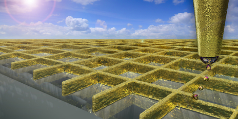
Image: Ben Newton/Digit Works
Poulikakos and his team are the first researchers to ever 3D print nanowalls like the ones used for touchscreen technology. The process will need to be further developed before it can be implemented on an industrial scale, but Poulikakos estimates that using gold and silver will actually be less expensive than indium tin oxide, as the metals do not require a cleanroom environment.
Once Nanodrip technology has been upscaled for industrial production, its potential applications include solar cells, which also require transparent electrodes with high conductivity – more conductive inks will allow for a much greater amount of energy to be harnessed. And, of course, there are our smartphones and tablets. I’m blaming my malfunctioning phone less on indium tin oxide and more on the fact that I bought the cheapest one I could find, but I’m hoping that maybe by the time I’m ready to buy a new one, the technology will be in place to allow touchscreens that respond at light speed.
The researchers recently published their findings in Advanced Materials, in a paper called ‘Electrohydrodynamic NanoDrip Printing of High Aspect Ratio Metal Grid Transparent Electrodes.’ Discuss this story in the Nanodrip 3D Printing forum thread on 3DPB.com
Subscribe to Our Email Newsletter
Stay up-to-date on all the latest news from the 3D printing industry and receive information and offers from third party vendors.
Print Services
Upload your 3D Models and get them printed quickly and efficiently.













You May Also Like
Bambu Lab Is Building More Than 3D Printers. Now Comes the S1 Scanner
Bambu Lab is moving into 3D scanning. The company has teased its upcoming Bambu Lab S1, its first 3D scanner, marking another step in its expansion beyond desktop 3D printers....
3D Printing News Briefs, October 14, 2026: Bolus, Aerospace Tooling, Water Filter, & More
In today’s 3D Printing News Briefs, we’re starting with medical news, as Myrava has received FDA 510(k) clearance for its 3D printed bolus. Moving on to aerospace and metals, AML3D...
The Hidden Economics of Powder Bed 3D Printing: Closing the Loop in Powder Management
Automation is a very topical thing in additive manufacturing at the moment. With renewed scale, some clients are fervently looking to automate production. Other business cases only make sense with...
10 Years of Multi Jet Fusion: Onsite at HP’s Vancouver, Washington Facility
At this year’s RAPID event in Boston, HP Additive Manufacturing Solutions celebrated ten years in the additive manufacturing (AM) market. The company ushered in the milestone with several innovations, including...