
Soon You’ll Roll Up Your 3D Printed, LE-OFET, Flexible Computer And Put It in Your Shirt Pocket

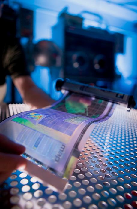
Organic Field-Effect Transistors (OFETs) were originally developed to produce extremely low-cost, large-area electronics aimed at producing printable and flexible electronic devices.
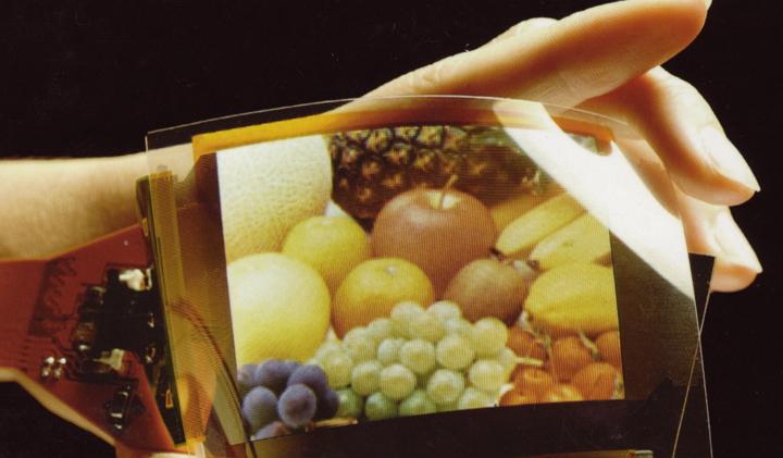
Researchers at Japan’s National Institute for Materials Science say improvements are now in the offing that will allow for the manufacture of transistors which can be used to make highly flexible and paper-thin computer screens and displays.
 They’re also sure to find applications in the world of 3D printing.
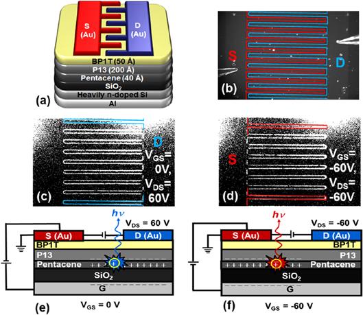
These photoactive organic field-effect transistors incorporate organic semi-conductors, can amplify weak electronic signals, and then either emit or receive light. And since their appearance on the scene in 2003, researchers say that enormous steps forward have been made in the development of one variant: light-emitting organic field-effect transistors (LE-OFETs).
 The photoactive OFETs are divided into two types; light-emitting (LE) and light-receiving (LR) OFETs. They are categorized according to functionality. The devices can function as non-volatile optical memories, phototransistors, and photochromism-based transistors.
In both cases a variety of configurations can produce devices like thin-film based transistors for practical applications and nanowiring.
And here’s where the technology gets truly interesting. Light-receiving organic field-effect transistors will break new ground for photonic and electronic devices and result in the creation of flexible displays where all the various device components (light-emitting elements, switching parts and the substrates) – are made of plastic materials.
For the most part, plastic materials mean “3D printable” materials.
As those materials have already been created and are expected to appear on the market in the near term, LE-OFETs are thought to be completely compatible with existing and popular electronic technologies.
 The Japanese researchers say the performance of devices which incorporate both light-emitting and light-receiving transistors is currently hampered by a number of issues, and that collaborative effort among organic chemists and device physicists will be required to resolve those stumbling blocks.
While the team say it may take ten years before all-plastic and highly flexible computing devices appear on the market, the technology is already attracting interest from a wide range of interested parties.
Yutaka Wakayama of the International Center for Materials Nanoarchitectonics (WPI-MANA) and the National Institute for Materials Science (NIMS) worked in conjunction with Ryoma Hayakawa and Hoon-Seok Seo on the research.
Can you see applications of OFET technology in the 3D printing sphere? Let us know your thoughts in the 3D Printed Flexible Computer forum thread on 3DPB.com.
Subscribe to Our Email Newsletter
Stay up-to-date on all the latest news from the 3D printing industry and receive information and offers from third party vendors.
Print Services
Upload your 3D Models and get them printed quickly and efficiently.


You May Also Like
Reinventing Reindustrialization: Why NAVWAR Project Manager Spencer Koroly Invented a Made-in-America 3D Printer
It has become virtually impossible to regularly follow additive manufacturing (AM) industry news and not stumble across the term “defense industrial base” (DIB), a concept encompassing all the many diverse...
Inside The Barnes Global Advisors’ Vision for a Stronger AM Ecosystem
As additive manufacturing (AM) continues to revolutionize the industrial landscape, Pittsburgh-based consultancy The Barnes Global Advisors (TBGA) is helping shape what that future looks like. As the largest independent AM...
Ruggedized: How USMC Innovation Officer Matt Pine Navigates 3D Printing in the Military
Disclaimer: Matt Pine’s views are not the views of the Department of Defense nor the U.S. Marine Corps Throughout this decade thus far, the military’s adoption of additive manufacturing (AM)...
U.S. Congress Calls Out 3D Printing in Proposal for Commercial Reserve Manufacturing Network
Last week, the U.S. House of Representatives’ Appropriations Committee moved the FY 2026 defense bill forward to the House floor. Included in the legislation is a $131 million proposal for...