
nScrypt’s Ken Church on Why Additive Electronics Is Finally Finding Its Fit

For years, additive manufacturing (AM) has promised to reshape electronics. The idea has always been to print circuits directly where they are needed, add them into parts, and move beyond flat circuit boards. But in practice, that promise has taken much longer to materialize than many expected. According to nScrypt CEO Ken Church, that delay was not due to a lack of ambition or investment, but something more fundamental.
“The cool factor carries you to a point. But not a sustainable point,” Church said. “Early demonstrations were impressive, often even spectacular, but they did not always translate into real-world performance or viable manufacturing. The industry could generate excitement, but it struggled to generate adoption.”
That’s a big part of what has held back additive electronics, Church told me during my visit to nScrypt’s headquarters in Orlando. The executive and AM industry veteran traces the roots of this effort back to the late 1990s, when DARPA began pushing for what would later be called additive electronics.
“At the time, the expectations were aggressive, even by DARPA standards. Researchers were asked to print fine-feature electronics, including resistors, capacitors, inductors, and antennas, on unconventional substrates such as paper, all while maintaining low temperatures and tight tolerances,” he recalled. “They said, we want 10 micron line widths. We want you to print on paper. We want resistors, capacitors, inductors, antennas, and batteries. That was 1999… super challenging.”
The funding was substantial, and the technical progress was real. But once those programs ended, the industry was left to stand on its own, and that is where reality set in.
“Materials were not yet ready. Performance did not match what engineers were used to. And perhaps most importantly, additive systems were not competing in a vacuum; they were competing against decades of refinement in traditional electronics manufacturing,” Church went on. “We sort of stubbed our toe. Our performance was not good.”
The gap was especially clear when it came to materials. Traditional electronics are built around copper, which has become the industry standard not because it is perfect, but because it is consistent, cost-effective, and deeply integrated into design and manufacturing workflows. Additive systems, in contrast, often relied on silver-based materials, which behave differently and come with their own tradeoffs.
“Industry was used to copper. All the design specifications were around the conductivity of copper. We mostly dealt in silver; it didn’t oxidize, but it’s considerably more expensive. That’s where things start to break down. Even when additive works, it doesn’t always match what engineers expect, because those expectations come from copper. So a lot of the time it’s being judged against standards it was never meant to meet,” Church explained. “If I tell you, ‘I could make that phone for you, but all you could do is call grandma,’ you’re gonna say, ‘that is so cool… but no thanks.’”
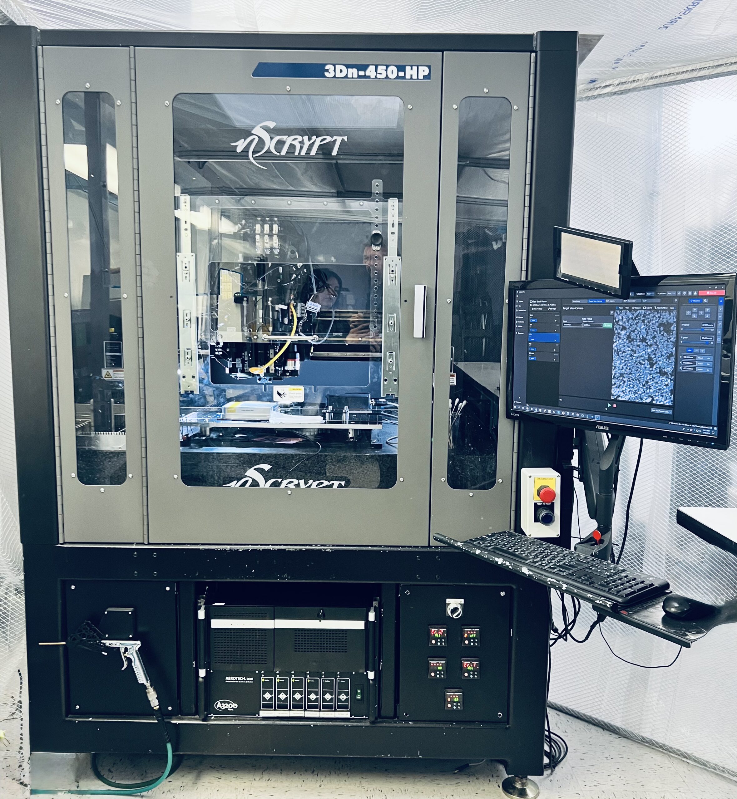
An nScrypt 3Dn-450-HP system, a “Factory in a Tool” (FiT) 3D manufacturing system designed for multi-material, high-speed, and high-resolution production.
Over time, that disconnect forced nScrypt to change how it approached the market. Instead of trying to replace traditional electronics completely, the company began focusing on where additive manufacturing could offer something fundamentally different.
“Whether we like it or not, we are competing with state-of-the-art. That realization led to a more grounded strategy for us, one that emphasized fit over ambition. Rather than attempting to replicate entire devices, we began identifying specific use cases where additive methods provide clear advantages.” Then he added, “How do you eat an elephant? One bite at a time. That’s how we look at it. Where do we fit? We fit one bite at a time.”
That idea has become something of a guiding principle for the company. Additive electronics won’t happen all at once; it will grow step by step, where it actually solves real problems.
And those “bites” show up where traditional electronics start to struggle. That includes things like printing on curved parts, flexible circuits, or building electronics into structures: things that flat boards just can’t do.
“The people we’re most successful with are the ones who have real pain points,” Church said. “They tell us, ‘We have a problem that a flat board can’t fix,’ and that’s when we say, ‘Okay, let’s talk.’”
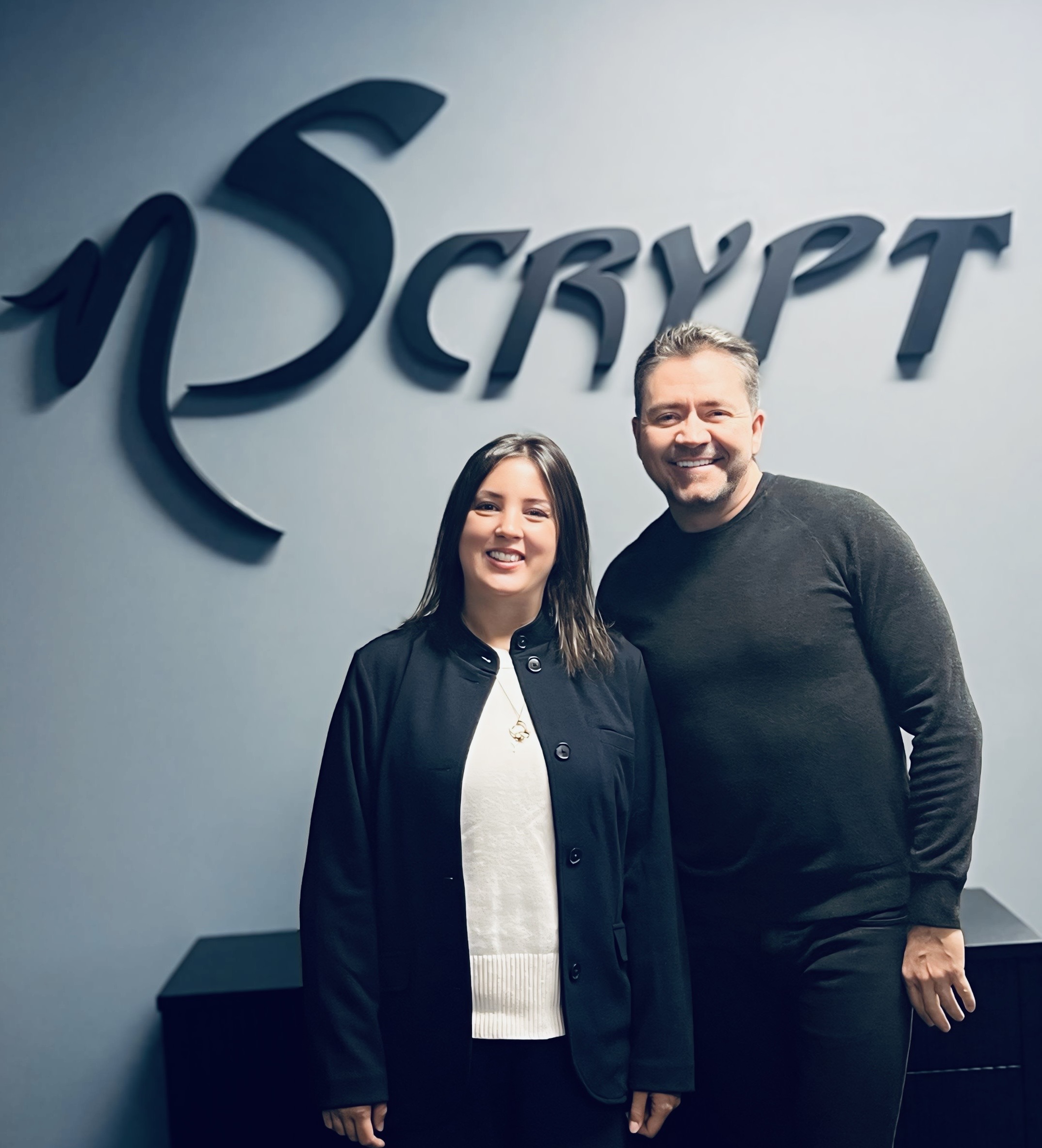
Ken Church and Vanesa Listek at nScrypt headquarters.
At the same time, Church is careful to define the limits of the technology. Not every application is a good fit, and not every problem should be approached with additive methods.
“If you need a million [dots] a second, then that’s not for us. That is not who we are. And that level of clarity is important in a field that has often been driven by broad claims.”
It too reflects a change in the message. Rather than positioning additive electronics as a “next generation” solution, nScrypt has begun framing it as something more immediate and practical.
Even with that shift, one of the biggest challenges is still the mindset. Engineers and designers are still trained within the constraints of traditional materials and processes. Their tools, their assumptions, and their expectations are all built around those systems, noted Church.
“All your designers learned how to design around copper. All your software was set around copper. When additive enters that environment, it is often judged against those same benchmarks, even when those benchmarks do not apply. We still make a great circuit,” he said. “But because we did not match your specifications, therefore, we were a failure.”
To move forward, Church argues that the industry needs to rethink how success is defined. Instead of asking whether additive matches traditional specifications, the more important question is whether it achieves the same functional outcome.
When those circuits work, whether they’re flat, flexible, or printed on a curve, the conversation starts to change. At that point, AM isn’t just a novelty; it becomes a real tool.
This article is the first in a three-part series based on 3DPrint.com’s visit to nScrypt’s headquarters in Orlando and conversations with Ken Church.
Images courtesy of 3DPrint.com
Subscribe to Our Email Newsletter
Stay up-to-date on all the latest news from the 3D printing industry and receive information and offers from third party vendors.
Print Services
Upload your 3D Models and get them printed quickly and efficiently.


You May Also Like
Harvard’s Jennifer Lewis Lab Is 3D Printing Artificial Muscles That Twist and Bend on Demand
Researchers at Harvard John A. Paulson School of Engineering and Applied Sciences (SEAS) have developed a new way to 3D print materials that can move on their own, bending, twisting,...
3D Printing News Briefs, May 2, 2026: Soft Robots, Agricultural Waste, & More
In this weekend’s 3D Printing News Briefs, we’ll start off with a multi-laser metal powder bed fusion 3D printer and post-processing news. We’ll end with research into soft robotics and...
Harvard SEAS Engineers Develop 3D Printing Method for Soft Robotic Components with Programmable Shapes
The world of soft robotics is still largely in its pure research phase, but the R&D landscape has started to produce examples of early-stage commercialization. Researchers have started to refine...
Boston’s Additive Edge: Harvard’s MEDscience Takes High Schoolers Into the Future of Medicine
Forget chalkboards and worksheets. At Harvard Medical School’s MEDscienceTECH Program, students learn medicine by building, coding, and experimenting – whether it’s navigating a LEGO robot through a 3D printed spine,...