
Optically Active Nanostructures 3D Printed by Austrian Research Team


For more than a decade, a research team at Austria’s Graz University of Technology has been developing a method for manufacturing nanostructures with 3D geometries. In November 2023, the team published an article in the journal Advanced Functional Materials, documenting two major breakthroughs they’d made on that front.
Titled “Spectral Tuning of Plasmonic Activity in 3D Nanostructures via High-Precision Nano-Printing”, the article by the Graz team details the use of focused electron beam induced deposition (FEBID) to create 3D structures from gold nanowires. Just as significantly, the team also demonstrated how they were able to use 3D simulation software to make the process more reliable and, therefore, more repeatable.
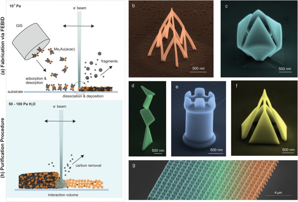
In a Graz University press release about the breakthroughs in 3D printed nanostructures, one of the research leads, Harald Plank, explained, “The biggest challenge in recent years was to transfer the 3D architectures into high-purity materials without destroying the morphology. This development leap enables new optical effects and application concepts thanks to the 3D aspect. By precisely controlling beam movements and exposure times, we are able to produce complex nanostructures with lattice- or sheet-like building blocks in a single step.” Regarding the software aspect, in particular, Plank said, “The consistency between simulations and real plasmonic resonances of a wide range of nanoarchitectures is very high. This is a huge step forward. The hard work of the last few years has finally paid off.”
The process works by putting a precursor material into the vacuum chamber of a Focused Ion Beam Scanning Electron Microscopy (FIB-SEM) device. At first, the precursor particles adhere to the chamber’s surface, after which they diffuse from one another and ultimately leave the surface. Use of a focused electron beam then yields the formation of metal deposits, with the process the team developed allowing them to create desired 3D shapes with individual features down to the sub-10 nm range.
Mention of “sub-10 nm” obviously immediately brings to mind the semiconductor sector, with that being the scale of features on the most advanced chips currently in production. The higher the performance of 3D printing at the nanoscale, the more that the 3D printing industry has to offer the semiconductor sector in terms of applications like advanced packaging and 3D printed electronics.
It is worth noting here that, around a month before the Graz University researchers published their results, researchers from China’s Tsinghua University published an article in the journal Science documenting their direct printing of semiconductors at the nanoscale. Against this background, the timing of electronic design automation (EDA) firm Synopsys’ in-progress acquisition of Ansys — said to be largely driven by chiplet design — becomes even more interesting.
While this is still clearly very much an R&D application, the semiconductor sector also represents perhaps the fastest track between R&D and commercialization of any industry in the global economy. Additionally, the fact that this specific application already has ten years of history behind it suggests it could start to be scaled up sooner rather than later.
Images courtesy of Advanced Functional Materials
Subscribe to Our Email Newsletter
Stay up-to-date on all the latest news from the 3D printing industry and receive information and offers from third party vendors.
Print Services
Upload your 3D Models and get them printed quickly and efficiently.


You May Also Like
Divergent Declares that German 3D Printers are Superior, And Plans Massive LPBF Expansion
Divergent has announced a new version of its Laser Powder Bed Fusion (LPBF) printer and a new site. The company aims to do nothing short of “further accelerating its mission...
Inside Haddy: Jay Rogers Wants 3D Printing to Build Real Products, Not Just Prototypes
A warehouse from the outside, but step inside Haddy and it shifts quickly: finished pieces up front, clean and minimal, furniture you can touch and sit on. Walking through the...
SpaceX IPO Puts a Major 3D Printing Powerhouse on Wall Street
SpaceX officially began trading on the Nasdaq today under the ticker symbol SPCX, marking one of the most anticipated and largest public offerings in Wall Street history. The company priced...
DEEP Manufacturing Collaborating with Fortius Metals to Demonstrate WAAM at Scale
DEEP Manufacturing is trying to build pressure vessels and marine habitats at scale with DED technology. Using commercial robot arms and wire arc additive manufacturing (WAAM), the company is hoping...