NASA’s Latest Mission Centers Around 3D Printed Circuits

NASA recently highlighted a successful space mission exploring the capabilities of hybrid 3D printed electronic circuits for NASA’s spacecrafts. The launch flew on April, 25th, 2023 and was led by NASA’s Goddard Space Flight Center’s aerospace engineer, Beth Pauette, and electronics engineer, Margaret Samuels. The results were promising, and could help NASA pack more technology into smaller spaces in future launches.
Missions like this are nothing new for NASA. Actually, this one was a part of NASA’s Suborbital Technology Experiment Carrier-9 (SubTEC9) rocket mission, a program created back in 2005 to test and demonstrate the functionalities of new/improved technology prior to space missions. For this mission, the spacecraft launched out of NASA’s Wallops Flight Facility near Chincoteague, Virginia, and explored the edge of space, reaching an altitude of 174 kilometers (108 miles) above sea-level. While the mission only lasted a few minutes, the team of scientists and engineers were able to gather valuable information about the electronic systems before the payload drifted back to Earth.
The main experiments centered around temperature and humidity sensors that were printed on the bay door and two attached panels. The sensors monitored the entire SubTEC9 rocket and relayed the data back to mission control. NASA’s team declared the tests a success and showed the spaced readiness of printed electronic technology and its ability to make payloads more efficient for future near-Earth and deep space missions.
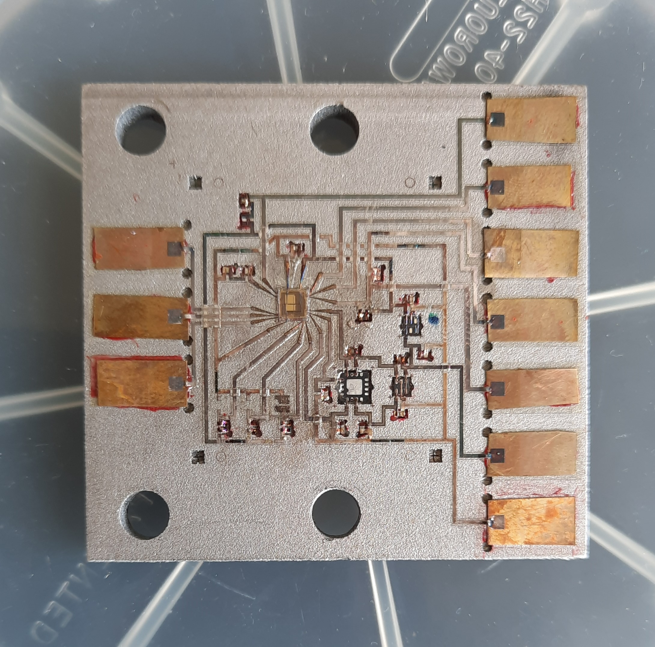
Picture of the 3D printed circuit used on the SubTEC9 mission flown on April 25, 2023. (Image courtesy of NASA/Karl B. Hille)
The inks and circuits used in this experiment were made by Pauette and Samuels’ colleagues at NASA’s Marshall Space Flight Center in Huntsville, AL and printed by Engineer Jason Fleischer from the University of Maryland’s Lab for Physical Sciences (LPS). The traces were printed at approximately 30 μm in width (about half the width of a human hair) and were able to be printed on any three-dimensional surface. By replacing traditional circuits with printed ones, the team hopes to not only condense the space needed for onboard electronics, but also mitigate the potential failure mechanisms seen in traditional circuit wire bonding and help make more precise antenna technology by increasing the angles at which a person can send and receive information in space.

Photo of the team showing the sensors with 3D printed circuits. Team lead Beth Paquette (left) stands with Jason Fleischer of the Laboratory for Physical Sciences (LPS), holding the curved metal plate with their printed electronics test assembly. Donghun Park, also with LPS, stands at right, while Wallops Electronics Engineer Brian Banks brings up the rear. (Image courtesy of NASA / Berit Bland)
“The uniqueness of this technology is being able to print a sensor actually where you need it. It’s a space saver. We can print on 3-dimensional surfaces with traces of about 30 microns – half the width of a human hair – or smaller between components. [This could] benefit many potential antennas and radio frequency applications.”
-Margaret Samuels, electronics engineer for NASA
It’s exciting to see the continued exploration of 3D printing’s potential applications towards space exploration. It was only two years ago when L3Harris announced that it had launched the first 3D printed circuit into space, and now the trend continues with this latest mission from NASA. Hopefully, the technology will continue to be used in the field, and if they continue seeing results similar to this experiment, the work is bound to continue well into the future.
Subscribe to Our Email Newsletter
Stay up-to-date on all the latest news from the 3D printing industry and receive information and offers from third party vendors.
Print Services
Upload your 3D Models and get them printed quickly and efficiently.


You May Also Like
The Dental Additive Manufacturing Market Could Nearly Double by 2033, According to AM Research
According to an AM Research report from 2024, the medical device industry, specifically in dentistry, prosthetics, and audiology, is expected to see significant growth as these segments continue to benefit from...
Heating Up: 3D Systems’ Scott Green Discusses 3D Printing’s Potential in the Data Center Industry
The relentless rise of NVIDIA, the steadily increasing pledges of major private and public investments in national infrastructure projects around the world, and the general cultural obsession with AI have...
AM Research Webinar Explores Continuum’s Sustainable Metal Additive Manufacturing Powders
Metal additive manufacturing (AM) powder supplier Continuum Powders is working to develop solutions that empower industries to reduce waste and optimize their resources. An independent life cycle assessment (LCA) of...
3D Printed Footwear Startup Koobz Lands $7.2M in Seed Round
California-based Koobz is focused on reshoring the U.S. footwear supply chain with advanced manufacturing processes, including 3D printing. The startup just announced that it has added $6 million to its...