
Korea’s Ulsan National Institute of Science and Technology: Exploring 3D & 4D Printing in Optics & Beyond


“Abundant new opportunities exist for exploration.”
Korean researchers from the Ulsan National Institute of Science and Technology are exploring more complex digital fabrication—and on two different levels, outlined in the recently published ‘3D and 4D printing for optics and metaphonics.’
The authors explore the latest progress made by researchers in both 3D and 4D printing, mainly as related to nanophotonics and metaphotonics, regarding materials, design, applications, and other areas such as reconfigurable structures.

Schematics of the 3D printing methods: Fused deposition modeling (FDM), PolyJet (or Material jetting), Direct ink writing (DIW), Stereolithography (SLA)/Digital light projector (DLP), Direct laser writing (DLW), Selective Laser Sintering (SLS).
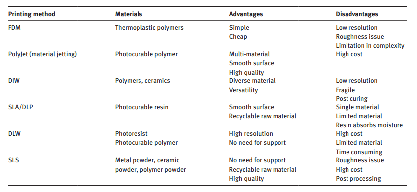
Comparison of 3D printing methods
As 3D printing becomes more accessible and more affordable around the world, users on many levels are becoming aware of the benefits, from greater speed and improved efficiency to the ability for customizing parts in nearly every related application—along with the potential for digital fabrication of much more complex, and highly functional, geometries.
Today, 3D printing is also used for creating optical components and metaphotonic structures—most importantly, without assembly required later. Optical parts can be put together along the ‘out-of-plane’ direction and can also be printed on nonplanar surfaces. The opportunities for customization may be limitless, and as designs are streamlined, waste of materials lessens significantly.
“Moreover, 3D printing can be useful for fabricating metaphotonic structures. Metaphotonics offers unprecedented control of electromagnetic fields in engineered materials and structures, in a manner not achievable with conventional optics,” state the researchers. “Therefore, metaphotonics often require nonconventional, complex 3D structures.”
4D printing certainly adds a fascinating twist to the world of digital fabrication, as materials may be surprisingly flexible and versatile, deforming as necessary (and as programmed, deeming them to be ‘smart materials’) and according to the environment—whether that may be humidity, temperature, or other factors. 4D active structures may be used in creating products like:
- Actuators
- Switches
- Sensors
- Deployable structures
- Soft robotics
- Medical devices
“Additionally, 4D printing can be applied to active optical and microwave structures,” state the researchers.
Functional materials for both 3D and 4D printing include:
- Embedded functional nanoparticles
- Filaments and inks for microwave antennas and components
- Smart materials for 4D printing
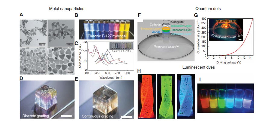
3D printing with functional nanomaterials. (A) TEM images of different sizes (15, 39, 58, 79 nm) of silver nanoprisms. (B) Photograph of Pluronic F-127 plasmonic inks with different sizes of silver nanoprisms. (C) Absorbance spectra (Inset shows the printed inks, scale bar: 5 mm). (D) Photograph of a discretely functionally graded 3D-printed plasmonic cube. (E) Photograph of a continuously functionally graded 3D printed plasmonic cube (scale bars: 5 mm). Adapted from Ref. [22]. Copyright (2017) John Wiley & Sons. (F) Schematic showing the QD-LED components printed on a curved surface. (G) Graph of current density vs. voltage of the 3D-printed QD-LED on a contact lens. The inset exhibits the electroluminescence from the 3D-printed QD-LED (scale bar: 1 mm). Reprinted from Ref. [23]. Copyright (2014) ACS Publications. (H) DLP printed complicated vases under the UV light illumination, which show luminescent red, green, and blue colors. (I) Photograph of the different luminescent color resins by blending. Reprinted from Ref. [24]. Copyright (2017) John Wiley & Sons.

Conductive materials for microwave applications. (A) Photograph of a 3D-printed antenna. (B) Reflection coefficient spectrum of the 3D-printed antenna. Reprinted from Ref. [26]. Copyright (2015) IEEE. (C) Picture of 3D-printed Mills-Cross cavity antennas. The left side is a receiving cavity and the right one is a transmitting cavity. (D) Synthesized composite apertures for imaging of a point-scatter array. (E) Reconstructed image of the array by the computational imaging algorithm. Reprinted from Ref. [27]. Copyright (2017) IEEE. (F) 3D printing of conductive scaffolds using a CNT/PLA solvent. (G) Graph of averaged EMI SE of the solid (i.e. filled) and scaffold patterns with different CNT loadings in the X-band range. Reprinted from Ref. [28]. Copyright (2017) Elsevier.
In terms of design and applications, the authors realize the ‘special advantages’ 3D and 4D printing hold over more conventional methods, although many manufacturers may still be reluctant to embrace such new technology. The use of freeform optical components is already becoming popular today though due to the benefits in numerous optical applications such as augmented reality and virtual reality.
“Recently, a parabolic mirror with nanometer-scale surface roughness (approximately 3 nm) was fabricated using SLA,” stated the researchers. “Its focused beam profile was almost identical to the beam from a mirror fabricated via conventional diamond milling.
“Optical parts were printed using SLA and a wax printer then, a polymer mixture gel composed of methacrylates, acrylates, and urethane-based polymers was coated and UV-cured.”

4D printing with smart materials. (A) 4D-printed structure that transforms its shape from a 1D line to a 3D cube. Adapted from Ref. [14]. Copyright (2014) John Wiley & Sons. (B) The shape memory process of the cubic frame made of carbon black doped polyurethane under light illumination of 87 mW/cm2. Adapted from Ref. [29]. Copyright (2017) John Wiley & Sons. Copyright (2016) Nature Publishing group. (C) 3D-printed structure that is mimicking the insect. The deformation behavior of the structure in a 30°C water is shown over time. The image on the lower right corner is the fully recovered structure in the 60°C water. Adapted from Ref. [16]. (D) Photographs of the shape memory assisted self-healing effect. Inserted pictures are the optical microscope images with a scale bar of 1 mm. Adapted from Ref. [30]. Copyright (2018) ACS Publications. (E) Hydrogel based 4D-printed structure (scale bar: 1 cm). Adapted from Ref. [31]. Copyright (2017) John Wiley & Sons. (F) Sequential deformation of a multi-material LCE structure. With molecular engineering, different actuation temperatures were realized (scale bar: 5 mm). Adapted from Ref. [32]. Copyright (2019) John Wiley & Sons. (G) 4D-printed structure that combined LCE with PDMS for adaptive optics. The pictures show the grid observed at different temperatures. Adapted from Ref. [33]. Copyright (2018) John Wiley & Sons.
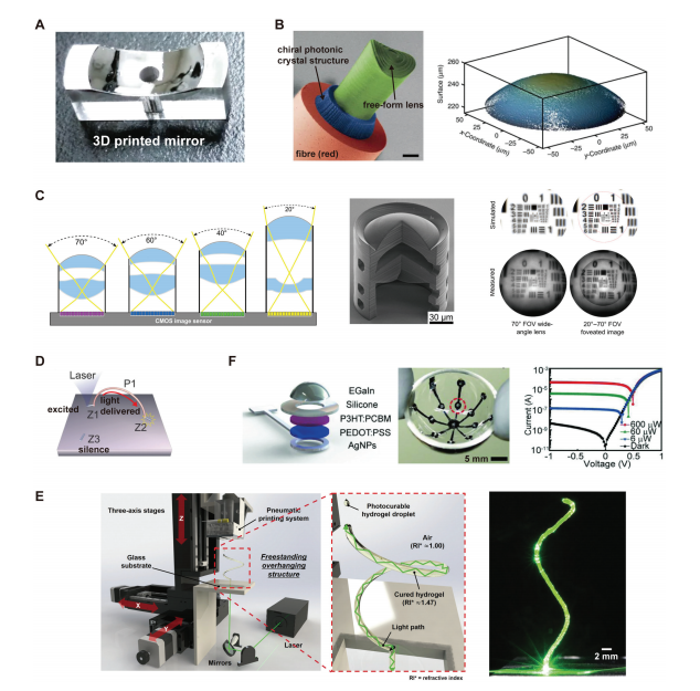
3D printing for optical and optoelectronic components. (A) 3D-printed parabolic mirror after smoothing and aluminum deposition. Adapted from Ref. [71]. Copyright (2018) Nature Publishing Group. (B) Left: Scanning electron microscope (SEM) image of a sub-micrometer optical element printed onto a single-mode fiber (scale bars: 25 μm). Right: Measured topography using optical interferometry of a spherical lens with a lens thickness of 250 μm, a radius of curvature 85.77 μm. Adapted from Ref. [72]. Copyright (2016) Nature Publishing Group. (C) Left: Four different FOV compound lenses on the same CMOS image sensor and the SEM image of a 3D-printed doublet lens. Right: Comparison of simulation and measurement images through a single compound lens with FOV of only a 70° (left), and with 20°, 40°, 60°, 70° (right). Adapted from Ref. [73]. Copyright (2017) AAAS. (D) Illustration explaining optical interconnection between two ZnO nanorods (Z1, Z2) through a polystyrene nanowire (P1). Adapted from Ref. [88]. Copyright (2016) John Wiley & Sons. (E) Left: Schematic view of the 3D printing system. The zoom-in part represents a 3D-printing method inspired by the light guide of an optical fiber. Right: Helical structure where light is guided and transmitted. Adapted from Ref. [75]. Copyright (2019) John Wiley & Sons. (F) Left: Schematic of the structure of the photodetector. Center: Photograph of the concentric photodetector array printed onto the inner surface of a hemispherical glass dome. Right: I-V characteristics of the photodetector onto the hemispherical glass dome. Adapted from Ref. [76]. Copyright (2018) John Wiley & Sons.
Optical waveguides and optoelectronic devices can be created, along with optical metamaterials, terahertz components, microwave metamaterials, and more.

3D printing for microwave metamaterials and transformation optics. (A) Diamond-like lattice composed of ABS only (right) and ABS + BaTiO3 composite (left). (B) Samples composed of alternating areas of ABS and ABS + BaTiO3 that are printed using a dual-extrusion nozzle. (C) Diamond-like lattice made of ABS with a 10 vol% NiZn ferrite filament. Adapted from Ref. [98]. Copyright (2015) The Royal Society Publishing. (D) PLA-SRRs sample after selective electroless plating on an ABS structure (inset: anti-resonant dispersion for bi-anisotropy). Adapted from Ref. [99]. Copyright (2017) AIP Publishing. (E) Left: Schematic of a GRIN lens with low (blue) and high (white) relative permittivity regions and photograph of the short horn with 3D-printed GRIN lens. Right: Experimental radiation pattern of the GRIN lens. Adapted from Ref. [100]. Copyright (2016) John Wiley & Sons (F) Photograph of a 3D-printed planar Luneberg lens. Adapted from Ref. [101]. Copyright (2018) ACS Publications. (G) 3D-printed Luneburg lens antenna (inset: schematic of the cubic-unit cell). Adapted from Ref. [102]. Copyright (2014) IEEE. (H) Photograph of a 3D-printed beam steering lens and the measured electric field distribution for the lens antenna. Adapted from Ref. [103]. Copyright (2016) IOP Publishing.
4D printing shows potential in a wide variety of applications but may offer special opportunity in creating optical and microwave structures, with the ability to transform nanophotonics and metaphotonics in:
- Active photonic devices
- Optical sensors
- Displays
- Antennas
“With biocompatible materials (such as hydrogels), implantable and stimuli-responsive photonic devices can be developed for biomedical applications,” concluded the researchers. “There are abundant new opportunities for investigation. For example, it was recently demonstrated that a dimer of aqueous beads induced strong field enhancement in the gap upon microwave incidence.
“Hydrogels consist of mostly water (>99%) and are commonly used in 4D printing. Thus, there could be interesting research opportunities involving the combination of stimuli-responsive functions with the microwave response in 3D-printed hydrogel structures.”

Future perspectives. (A) Schematic for metal-ink 3D printing with IR laser sintering. (B) freestanding helical coils (diameter: 500 μm). (C) Printed butterflies with freestanding wings. Adapted from Ref. [138]. Copyright (2016) National Academy of Sciences. (D) Plasma is formed between two grape (or hydrogel) beads, because of strong microwave field enhancement in the gap. Adapted from Ref. [139]. Copyright (2019) National Academy of Sciences.
“Our review can be helpful for researchers in the nanophotonics and metaphotonics communities who wish to learn about recent ideas and developments in 3D and 4D printing.”
What do you think of this news? Let us know your thoughts; join the discussion of this and other 3D printing topics at 3DPrintBoard.com.
[Source / Images: ‘3D and 4D printing for optics and metaphonics’]Subscribe to Our Email Newsletter
Stay up-to-date on all the latest news from the 3D printing industry and receive information and offers from third party vendors.
Print Services
Upload your 3D Models and get them printed quickly and efficiently.


You May Also Like
3D Printing News Briefs, June 13, 2026: Management Changes, Project Calls, & Wheelchairs
We’ll kick this weekend’s 3D Printing News Briefs off with some advisory board and management changes, and then move on to project call news. We’ll end with some heartwarming stories...
Researchers Combine AI and Bioprinting to Create Tiny Blood Vessel Networks
If 2026 has a theme in bioprinting, it may be blood vessels. Researchers can already print incredibly sophisticated tissues. The harder part is keeping those tissues alive. Without a network...
University of Arkansas Researchers Test Metal 3D Printing in a Mars-Like Atmosphere
If humans eventually establish a long-term presence on Mars, they will face a major manufacturing challenge almost immediately. Tools will break. Parts will wear out. Equipment will need repairs. But...
UT Researchers Use 3D Printing to Develop “Tabletop EUV Lithography” Process
Photolithography, the semiconductor manufacturing process whereby lasers transfer patterns onto chemical layers coating a substrate, is one of the most amazing industrial processes humanity has ever created. It is also...