
Multimaterial 3D Printing Filaments for Optoelectronics

Authors Gabriel Loke, Rodger Yuan, Michael Rein, Tural Khudiyev, Yash Jain, John Joannopoulous, and Yoel Fink have all come together to explore new filament options, with their findings outlined in the recently published ‘Structured multimaterial filaments for 3D printing of optoelectronics.’
While 3D printing of ‘disparate materials’ such as metals, plastics, and semiconductor device interfaces continues to be difficult (for high-resolution production), the authors explore filaments in complex microstructures meant to promote improved manufacturing. There are current limits due to issues with:
- Lack of bonding
- Delamination due to differences in material
- Inferior functionality
- Poor conductivity
- Wetting of ink
- Degradation in prints
- Distortion in structure
- Extended production time
The authors were able to create a range of multi-material filament inks for developing hierarchical 3D functional systems, allowing for greater control and use of interchangeable materials. Pre-forms were drawn into continuous ‘kilometers-long microstructured filaments,’ suitable for FDM 3D printing. Functionality from the filament to a 3D printed object occurs here with a printable pixelated electroluminescent light-emitting filament containing:
- Metallic BiSn core
- Electrically-conducting W
- Electroluminescent ZnS
- Insulating cladding PC surrounded by a print adhesion tie layer COC
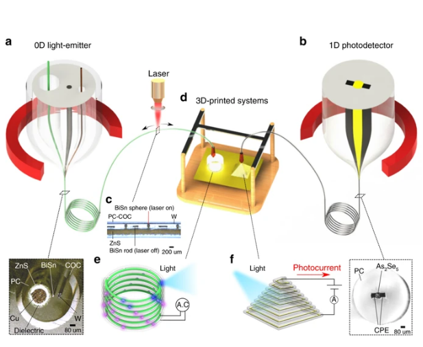 Discrete microspheres help to form the spatial light-emitters, while the BiSn microsphere mixed with ZnS and W allows for the 0-dimensional electroluminescent pixel in a 3D printed macrostructure.
“To form these spheres, the BiSn core confined within the transparent viscoelastic PC matrix is subjected to laser-induced capillary breakup34,35, which transforms the core into thermodynamically-stable BiSn spheres. As the sphere has a larger diameter than its core, the distance between the W and ZnS wires is bridged, forming interfacial electrical connections between BiSn and W, as well as, BiSn and ZnS,” state the researchers.
“By connecting W and Cu to an alternating voltage source, these electrically conductive spheres link the electric potential from W towards the outer surface of ZnS, enabling sufficient electric field strength to induce light emission from the ZnS layer via electroluminescence.”
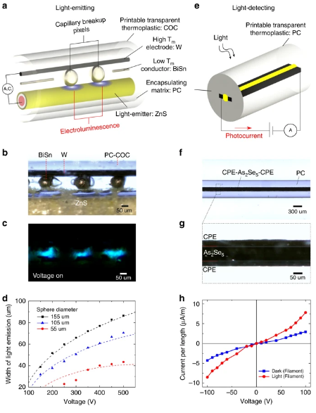
Characterization of the Optoelectronic Filaments. a Schematic of the pixelated light-emitting filament, illustrating the filament design for light-emission. b Optical micrograph of the in-filament low melting-point (Tm) BiSn conductive spheres electrically interfacing high melting-point W and ZnS. c Electroluminescent light-emission from ZnS at distinct sphere locations in (b). d Plot of width of light-emission versus AC voltage for different sphere sizes. The plotted dotted lines are derived from the theoretical framework presented in Supplementary Note 1. e Schematic of the light-detecting filament, with an external circuit connected to opposite ends of the different electrodes. f, g Planar optical micrographs of long-distance intimate electrical contact between CPE and As2Se5, which contributes to h generation of photocurrent upon light impingement. Both filaments are cladded by a printable thermoplastic (COC or PC) and contain functional interfaces between disparate materials classes immobilized by a PC matrix
The structures are beneficial since light can be detected at high resolution, fully closed structures can sense light, and they can also work for applications like tracking satellites or energy harvesting. This type of printing works with a wide range of multi-material filaments, where the core can mix disparate materials for creating a variety of functionalities. Brittle materials possessing a wide core diameter can be 3D printed in low curvature turns; however, they are not able to handle high bending strains.
Filament material is made up of a functional domain with an active light-emitting wire, topped by an 18 µm-thick dielectric, and capped by an 18 µm-thick electroluminescent (EL) ZnS-phosphor outer layer.
“A conductive tungsten electrode (diameter of 50 µm) is spaced 0.05–0.1 mm away from the ZnS, and a 40 µm-diameter conductive BiSn cylindrical core is centrally situated with no connection to tungsten and ZnS,” state the researchers. “The 0.5–0.7 mm diameter material polycarbonate (PC) holds all of these materials and interfaces in position. Lastly, a 0.2–0.4 mm thick cyclic olefin copolymer (COC), which envelopes the cylindrical polycarbonate core, serves as the printable thermoplastic.”
The printer used in the study was a Rova3D, along with a hot end with a stainless-steel tube ranging up to 2mm long, heated by nichrome wire. For the study, the team fabricated an airplane wing, created with light-emitting filament at the top, and then three layers of photo-detecting filaments.
The study of materials has become intensive in the 3D printing world, and especially as users strive to add multiple materials and colors, from use in Air Jet DLP processes to SLA/DLP to use with new extruders. What do you think of this news? Let us know your thoughts; join the discussion of this and other 3D printing topics at 3DPrintBoard.com.
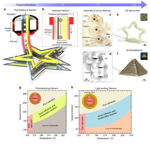
Multiscale Print Process. a The microstructured multimaterial filament is fed quickly through a short hot end. Precision of the print can be enhanced by using hot end and filaments of smaller diameters. b Filament surface heating (FSH) generates a surface-heated effect with the filament surface temperature rising beyond its critical fusing temperature (Tcrit) while maintaining the temperature of the inner encapsulating polymer at a temperature below its glass transition (Tg). Microscale features within the ink can be precisely arranged for varying functionalities. c, d Cross-sectional optical micrographs showcasing a hierarchical assembly of millimeter-scale fused lines containing interfacial microstructures of different material classes. These assembly can be further stacked and shaped into three-dimensional centimeter-scale objects like e a star and a f pyramid which are printed from the light-emitting and light-detecting filaments, respectively, via FSH. Speed-temperature plots for the printing of g PC-cladded light-detecting and h COC-clad/PC-core light-emitting filaments
Subscribe to Our Email Newsletter
Stay up-to-date on all the latest news from the 3D printing industry and receive information and offers from third party vendors.
Print Services
Upload your 3D Models and get them printed quickly and efficiently.


You May Also Like
The Dental Additive Manufacturing Market Could Nearly Double by 2033, According to AM Research
According to an AM Research report from 2024, the medical device industry, specifically in dentistry, prosthetics, and audiology, is expected to see significant growth as these segments continue to benefit from...
Heating Up: 3D Systems’ Scott Green Discusses 3D Printing’s Potential in the Data Center Industry
The relentless rise of NVIDIA, the steadily increasing pledges of major private and public investments in national infrastructure projects around the world, and the general cultural obsession with AI have...
AM Research Webinar Explores Continuum’s Sustainable Metal Additive Manufacturing Powders
Metal additive manufacturing (AM) powder supplier Continuum Powders is working to develop solutions that empower industries to reduce waste and optimize their resources. An independent life cycle assessment (LCA) of...
3D Printed Footwear Startup Koobz Lands $7.2M in Seed Round
California-based Koobz is focused on reshoring the U.S. footwear supply chain with advanced manufacturing processes, including 3D printing. The startup just announced that it has added $6 million to its...