New 3D Printing Approach Enables More Complex Electrical Routing for 3D Integration of Microelectronic Subsystems


Demand for higher resolution and high-precision parts is driving the evolution of additive manufacturing. The latest 3D printer design from Boston Micro Fabrication (BMF) uses a new approach called Projection Micro Stereolithography (PµSL), which is capable of printing polymer parts with 2µm resolution — unprecedented metrics in 3D printing. PµSL enables mold-free, ultra-high-resolution, fast prototyping, and end-part capability not possible before.
BMF globally launched their line of commercial micro-precision 3D printers in 2020, and using BMF’s microArch S130 model, HRL Laboratories, LLC, has now demonstrated ceramic interposers with previously impossible slanted and curved vias with diameters of less than 10µm. Vias are small openings in insulating layers that allow conductive connections between semiconductor layers in integrated circuits.
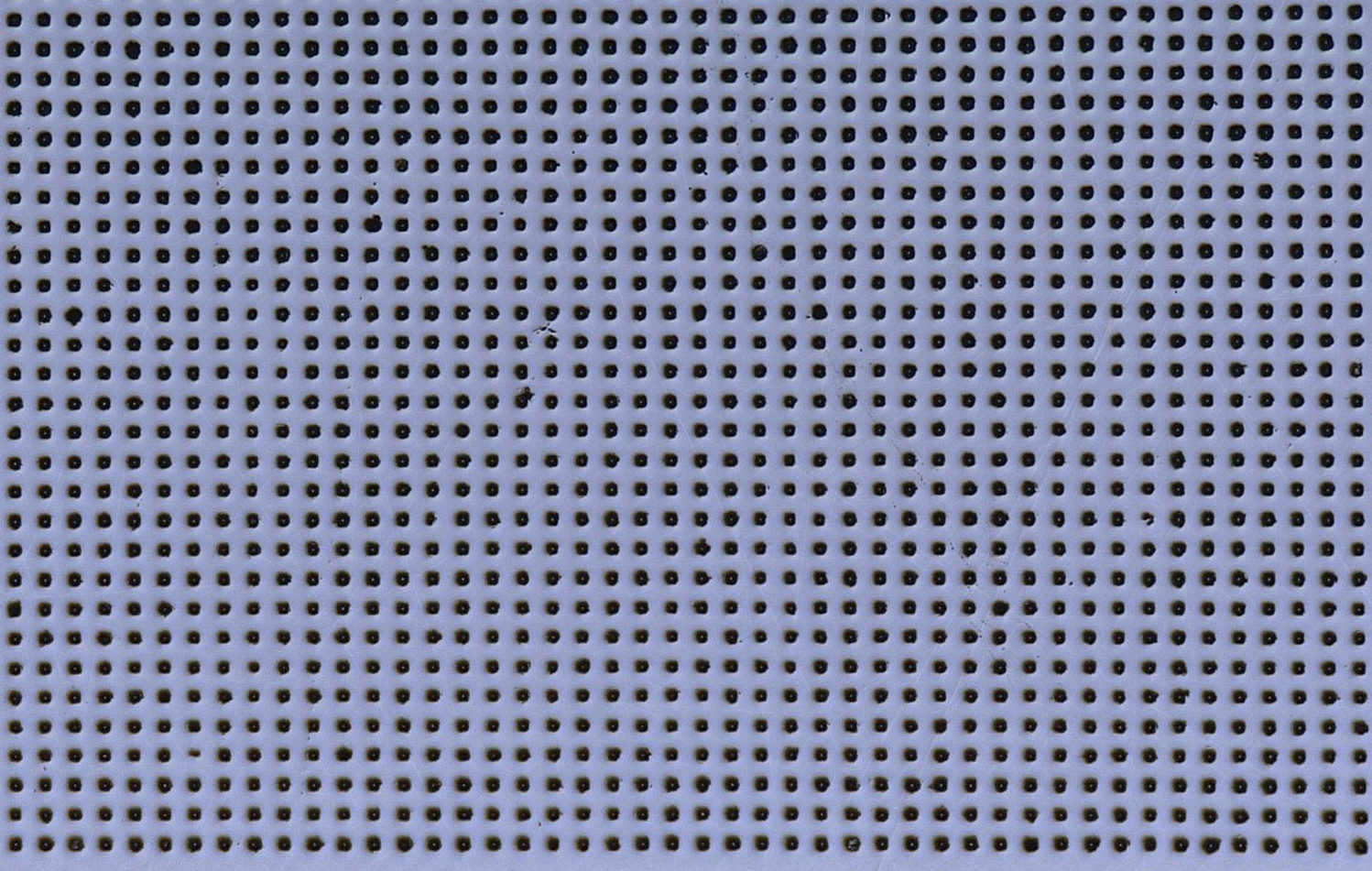
Figure 1: 3D printed via array with 10um holes spaced at 20um pitch in ceramic.
“We have printed arrays of straight, slanted, and curved vias and have not hit a limit in aspect ratio yet with the low-viscosity ceramic resin that we developed in house,” said HRL Lead Engineer Kayleigh Porter. PµSL additive manufacturing now offers nearly limitless possibilities for routing vias. After being printed in ceramic, the vias are metallized to electrically connect different devices and integrated circuits.
“We are developing this technology to improve 3D integration of microelectronic subsystems such as infrared cameras and radar receivers,” said HRL group manager Dr. Tobias Schaedler. “Smaller, lighter, and more power-efficient system designs are currently limited by electrical routing and packaging, but our additive technology could resolve this bottleneck.”
With conventional semiconductor processing methods such as chemical etching, only straight vias can be fabricated. Larger holes can be drilled at angles, but no drilling approach can realize vias with curvature.
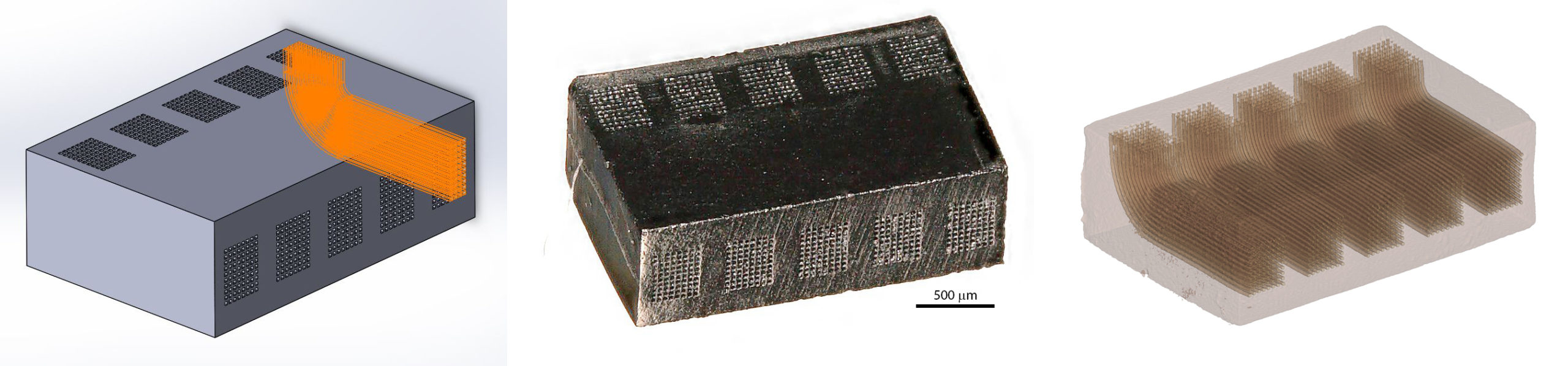
Figure 2: Computer Aided Design of part with curved vias, 3D printed ceramic part. Micro x-ray computer tomography image of curved vias in ceramic.
“We are very excited to collaborate with HRL on this project,” said BMF CEO John Kawola. “The level of resolution, accuracy, and precision that can be achieved at speeds suitable for production made BMF’s microArch S130 the perfect choice for HRL’s project. BMF is constantly working to push the limits of what can be achieved and we will continue to work with HRL and our other customers to meet the needs that their projects demand.”
HRL Laboratories’ development effort is currently funded by DARPA’s Microsystems Technology Office under the Focal arrays for Curved Infrared Imagers (FOCII) program.
Subscribe to Our Email Newsletter
Stay up-to-date on all the latest news from the 3D printing industry and receive information and offers from third party vendors.
Print Services
Upload your 3D Models and get them printed quickly and efficiently.


You May Also Like
From Vision to Reality: Secure Additive Manufacturing for Brazil’s Energy Sector
In the oil and gas industry, every day of unplanned downtime can translate into significant operational and financial losses. When a critical component is unavailable, operators may wait days or...
3YOURMIND Partners with Phillips Corp. in US Navy’s RIMPAC Distributed Manufacturing Experiment
I recently wrote about the US Navy’s development of the Advanced Integrated Mobile Machine Shop (AIMMS), a containerized unit built around the Phillips Additive Hybrid system, which combines DED and...
Inside Haddy: Jay Rogers Wants 3D Printing to Build Real Products, Not Just Prototypes
A warehouse from the outside, but step inside Haddy and it shifts quickly: finished pieces up front, clean and minimal, furniture you can touch and sit on. Walking through the...
3D Printing & the Autonomous Era: Defense Tech’s Latest Mutation
When we last checked in on the broad defense tech landscape and the role of the additive manufacturing (AM) industry in that environment, it became clear that the connecting thread...