3D Printing & Conductivity: Preparing New Polymer Bioinks for Electronics & Other Applications


International researchers delve into the area of materials science and 3D printing—a common theme today—but in this study, conductivity is the focus. Detailing their findings in the recently published ‘3D Printing of Conducting Polymers,’ the authors make it clear that while such polymers offer great potential in applications like electronics, there have still been challenges to overcome.
Upon developing a high-performance conducting polymer ink based on poly(3,4-ethylenedioxythiophene):polystyrene sulfonate (PEDOT:PSS), the researchers aimed to create a concentrated solution of nanofibrils.

a, b, Pristine PEDOT:PSS solution (a) can be converted into a 3D printable conducting polymer ink (b) by lyophilization in cryogenic condition and rdispersion with a solvent. c, 3D-printed conducting polymers can be converted into a pure PEDOT:PSS both in dry and hydrogel states by dry-annealing and subsequent swelling in wet environment, respectively. d CryoTEM image of a pristine PEDOT:PSS solution. e CryoTEM image of a 3D printable conducting polymer ink. f TEM image of a dry-annealed 3D-printed conducting polymer. g–j Images of re-dispersed suspensions with varying PEDOT:PSS nanofibril concentration. k SAXS characterization of conducting polymer inks with varying PEDOT:PSS nanofibril concentration. The d-spacing L is calculated by the Bragg expression L = 2π/qmax. l Apparent viscosity as a function of shear rate for conducting polymer inks of varying PEDOT:PSS nanofibril concentration. m Apparent viscosity of conducting polymer inks as a function of PEDOT:PSS nanofibril concentration. n Shear storage modulus as a function of shear stress for conducting polymer inks of varying PEDOT:PSS nanofibril concentration. o Shear yield stress of conducting polymer inks as a function of PEDOT:PSS nanofibril concentration. For TEM images in (d–f), the experiments were repeated (n = 5) based on independently prepared samples with reproducible results. Scale bars, 100 nm.
With ‘superior printability,’ the polymer ink offers a range of high-performance capabilities, printing with:
- High resolution
- High aspect ratio
- Overhanging structures
In this study, the researchers created print mesh samples of the ink via 200-, 100-, 50-, and 30-µm diameter nozzles. The structures could be easily transformed into dry or hydrogel form, with ‘long-term stability’ to be expected wet environments without degradation—even after storing for six months.
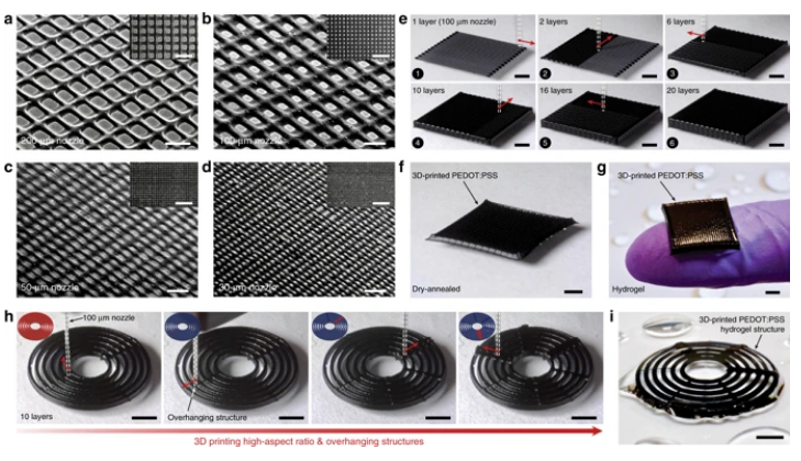
a–d SEM images of 3D-printed conducting polymer meshes by 200-µm (a), 100-µm (b), 50-µm (c), and 30-µm (d) nozzles. e Sequential snapshots for 3D printing of a 20-layered meshed structure by the conducting polymer ink. f 3D-printed conducting polymer mesh after dry-annealing. g 3D-printed conducting polymer mesh in hydrogel state. h Sequential snapshots for 3D printing of overhanging features over high aspect ratio structures by the conducting polymer ink. i 3D-printed conducting polymer structure with overhanging features in hydrogel state. Scale bars, 500 µm (a); 200 µm (b–d); 1 mm (a–d, inset panels); 2 mm (e–i).
The ink can also be integrated into multi-material 3D printing processes easily, proven during the study as the team created a structure similar to a high-density multi-electrode array (MEA) based on multi-material 3D printing of the conducting polymer ink and an insulating polydimethylsiloxane (PDMS) ink—all within 30 minutes.
“The 3D printed MEA-like structure shows a complex microscale electrode pattern and a PDMS well that are comparable to a commercially available MEA fabricated by multi-step lithographic processes and post-assembly,” stated the researchers.
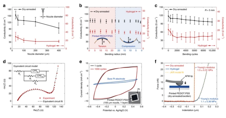
a Conductivity as a function of nozzle diameter for 3D-printed conducting polymers in dry and hydrogel states. b Conductivity as a function of bending radius for 3D-printed conducting polymers in dry (17 µm, thickness) and hydrogel (78 µm, thickness) states. PI indicates polyimide. c Conductivity as a function of bending cycles for 3D-printed conducting polymers in dry (17 µm, thickness) and hydrogel (78 µm, thickness) states. d Nyquist plot obtained from the EIS characterization for a 3D-printed conducting polymer on Pt substrate (78 µm, thickness) overlaid with the plot predicted from the corresponding equivalent circuit model38. In the equivalent circuit models, Re represents electronic resistance, Ri represents ionic resistance, Rc represents the total ohmic resistance of the cell assembly, CPEdl represents the double-layer constant phase element (CPE), whereas CPEg represents the geometric CPE. CPE is used to account inhomogeneous or imperfect capacitance and are represented by the parameters Q and n where Q represents the peudocapacitance value and n represents the deviation from ideal capacitive behavior. The true capacitance C can be calculated from these parameters by using the relationship C = Qωmaxn−1, where ωmax is the frequency at which the imaginary component reaches a maximum37. The fitted values for 3D-printed PEDOT:PSS are Re = 107.1 Ω, Ri = 105.5 Ω, Rc = 14.07 Ω, Qdl = 1.467 × 10⁻⁵ F sn−1, ndl = 0.924, Qg = 4.446 × 10⁻⁷ F sn−1, and ndl = 0.647. e CV characterization for a 3D-printed conducting polymer on Pt substrate. f Nanoindentation characterizations for 3D-printed conducting polymers in dry and hydrogel states with the JKR model fits. Values in (a–c) represent the mean and the standard deviation (n = 5 per each testing conditions based on independently prepared samples and performed experiments).
Because the polymers are highly reproducible, they can be 3D printed quickly with over 100 circuit patterns in less than 30 minutes, displaying ‘high electrical conductivity.’ This type of production offers an alternative to ink-jet or screen printing—along with greater versatility in design options, depending on required applications.
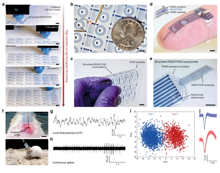
a Sequential snapshots for 3D printing of high-density flexible electronic circuit patterns by the conducting polymer ink. b Lighting up of LED on the 3D-printed conducting polymer circuit. PETE indicates polyethylene terephthalate. c Bending of the 3D-printed conducting polymer circuit without failure. d Image of the 3D-printed soft neural probe with 9-channels by the conducting polymer ink and the PDMS ink. e Image of the 3D-printed soft neural probe in magnified view. f Images of the implanted 3D-printed soft neural probe (top) and a freely moving mouse with the implanted probe (bottom). g, h Representative electrophysiological recordings in the mouse dHPC by the 3D-printed soft neural probe. Local field potential (LFP) traces (0.5 to 250 Hz) under freely moving conditions (g). Continuous extracellular action potential (AP) traces (300 to 40 kHz) recorded under freely moving conditions (h). i Principal component analysis of the recorded single-unit potentials from (h). j Average two units spike waveforms recorded over time corresponding to clusters in (i). Scale bars, 5 mm (a–c); 1 mm (d, e); 2 mm (f).
Experiments were performed using a customized Cartesian gantry style 3D printer by Aerotech, offering a variety of nozzle sizes. Conductivity was measured in the 3D printed polymers as the researchers employed a four-point probe. Samples were prepared via one layer of conducting polymer ink printed into a rectangular shape of 30 mm in length and 5 mm in width, featuring 100-µm nozzles on glass substrates, and copper wire electrodes attached with silver paste to the surfaces.
“This work not only addresses the existing challenges in 3D printing of conducting polymers but also offers a promising fabrication strategy for flexible electronics, wearable devices, and bioelectronics based on conducting polymers,” concluded the researchers.
3D printing and electronics accompany each other—whether in the form of newly developed composites for greater functionality, in use with smart textiles, circuit boards, or other useful technologies. Experiments and innovations regarding 3D printing and conductive materials are becoming increasingly popular too as users, researchers, and manufacturers look for better ways to create more powerful parts.
What do you think of this news? Let us know your thoughts! Join the discussion of this and other 3D printing topics at 3DPrintBoard.com.
[Source / Images: ‘3D Printing of Conducting Polymers’]Subscribe to Our Email Newsletter
Stay up-to-date on all the latest news from the 3D printing industry and receive information and offers from third party vendors.
Print Services
Upload your 3D Models and get them printed quickly and efficiently.


You May Also Like
The Drone Industry is Showing Where 3D Printing Delivers Real Value, AM Research Report Finds
The rapid rise of drones is creating one of the biggest opportunities for additive manufacturing (AM). Whether they’re used on battlefields, inspecting bridges or crops, or delivering supplies, drones need...
3D Printing News Briefs, June 27, 2026: Nanoscale 3D Printing, Defense Readiness, & More
We’re starting with a story about a grant for advanced nanoscale 3D printing in this weekend’s 3D Printing News Briefs, and then on to metal additive manufacturing (AM) for defense...
US Army Awards Continuous Composites 3D Printed Missile Component Contract
Despite the very loud, indignant claims from American defense officials that the US hasn’t depleted a significant portion of its munitions stockpiles, the US has depleted a significant portion of...
Rheinmetall Uses Ducting Made with Minifactory for Challenger 3 Tanks
Rheinmetall UK is using Minifactory Material Extusion as the primary production method for tank ducting on the Challenger 3 Main Battle Tank program. The Challenger 3 is the UK’s formidable...