EPFL Researchers 3D Print Atomic Microscopy Sensors at the Nanoscale


![]() Thanks to 3D printing, the world of high-resolution microscopy is about to be elevated further. Delving into those nanos (smaller than small) that we hear so much about today, and often in relevance to 3D technology, researchers at EPFL’s Laboratory for Bio- and Nano-Instrumentation have been busy using them in developing both the microscopy sensor—and the cantilever—of the future.
Thanks to 3D printing, the world of high-resolution microscopy is about to be elevated further. Delving into those nanos (smaller than small) that we hear so much about today, and often in relevance to 3D technology, researchers at EPFL’s Laboratory for Bio- and Nano-Instrumentation have been busy using them in developing both the microscopy sensor—and the cantilever—of the future.
All outlined in a recent paper, ‘Direct-write nanoscale printing of nanogranular tunnelling strain sensors for sub-micrometre cantilevers,’ by Maja Dukic, Marcel Winhold, Christian H. Schwalb, Jonathan D. Adams, Vladimir Stavrov, Michael Huth & Georg E. Fantner, the research team discusses their latest achievement in using 3D printing at the nanoscale to make a 5-nanometer thick sensor for their specialized cantilevers, as well as real world applications they’ve already been able to put the sensors to work in for atomic force microscopy.
“Using our method, the cantilever can be 100 times smaller,” says Georg Fantner, the lab’s director.
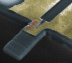
Example of nanogranular tunnelling resistor (NTR) deposited on a 1 μm wide, 300 nm thick free standing SiN cantilever [Image: EPFL]
“The sensors can be deposited with lateral dimensions down to tens of nm, allowing the readout of nanoscale cantilevers without constraints on their size, geometry or material,” state the researchers in their paper.
“By modifying the inter-granular tunnel-coupling strength, the sensors’ conductivity can be tuned by up to four orders of magnitude, to optimize their performance. We show that the nanoscale printed sensors are functional on 500 nm wide cantilevers and that their sensitivity is suited even for demanding applications such as atomic force microscopy.”
Both material and size were a big consideration as they embarked on making the new sensors. Working with Michael Huth’s lab at Goethe University Frankfurt, the researchers were able to create sensors fabricated with platinum nanoparticles, highly conductive and surrounded by a carbon matrix that acts as an insulator. They found, however, that in dealing with nanomaterials, some electrons could actually make their way through the insulation and then journey from one nanoparticle to another.
“It’s sort of like if people walking on a path came up against a wall and only the courageous few managed to climb over it,” says Fantner.
The team discovered that as the sensors’ shape is transformed, nanoparticles separate further and further from each other, with less of the electron jumping activity.
They also went on to discuss how one of the more unique and ‘extraordinary’ features of the sensors is that they are so scalable in both height and width.
“Minimizing the thickness and width of the sensing element is also crucial to maintain a high signal from a strain-sensing element in a nano-cantilever. The sensor should be thin enough as to not contribute much to the flexural rigidity of the cantilever. This is especially problematic for nano-cantilevers intended for the measurement of small forces at high bandwidths (such as cantilevers for HS-AFM).”
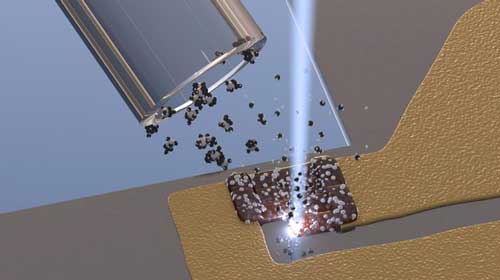
The sensors are made with platinum nanoparticles surrounded by an insulating carbon matrix. [Image: EPFL]
“In a vacuum, we distribute a precursor gas containing platinum and carbon atoms over a substrate. Then we apply an electron beam. The platinum atoms gather and form nanoparticles, and the carbon atoms naturally form a matrix around them,” said Maja Dukic, the article’s lead author. “By repeating this process, we can build sensors with any thickness and shape we want. We have proven that we could build these sensors and that they work on existing infrastructures. Our technique can now be used for broader applications, ranging from biosensors, ABS sensors for cars, to touch sensors on flexible membranes in prosthetics and artificial skin.”
Discuss further in the 3D Printed Microscopy Sensors forum over at 3DPB.com.
[Sources: Nano Werk; Nature Communications]
Subscribe to Our Email Newsletter
Stay up-to-date on all the latest news from the 3D printing industry and receive information and offers from third party vendors.
Print Services
Upload your 3D Models and get them printed quickly and efficiently.


You May Also Like
GKN Aerospace & Pratt & Whitney to Use Additive for the F135 Engine
GKN Aerospace and RTX unit Pratt & Whitney will collaborate on additive manufacturing for the F135 engine. This is an important engine. The turbofan powers the F-35 Lightning II, but...
Zaha Hadid Architects Print 6M Model with WASP’s Robotic Arm Solutions
Zaha Hadid Architects (ZHA) have successfully used WASP 3D printers to make a 6-meter-tall model of an aircraft control tower. Zaha Hadid Architects’ Tech Lab made the tower in-house for the ZHAviation...
3DPOD 303: 6K Additive CEO Frank Roberts on Premium and Sustainable Metal AM Powder
6K Additive is roaring ahead with a recycling solution for metals. Their path from scrap to powder is helping the US to be more resilient, produce powder locally and perhaps...
3D Printing News Briefs, June 18, 2026: Reseller, Relocation, Metal Space Powder, & More
We’ll start with business news in today’s 3D Printing News Briefs, as XJet appointed a value-added reseller in Germany, BIO INX is expanding its presence in the Italian market, and...