
3D Printing Steps in to Aid Semiconductor Industry’s Faltering Supply Chains

At this point in its evolution, additive manufacturing (AM) is growing far beyond the aerospace sector that kickstarted its adoption for end part production. It is being incorporated into automotive, general industry, energy and more. This includes the semiconductor industry, where complex machinery can benefit from some of the same advantages that AM brings to other sectors, such as improved efficiency, production on demand, and innovative design possibilities. To learn more, we spoke to Scott Green, Principal Solutions Leader for semiconductors at 3D Systems.
While there are about five leading chip makers— Intel, Samsung, NVIDIA, Texas Instruments, and Broadcom—they rely on an extensive line of contractors and subcontractors and system suppliers to make each individual component that lands on the final board, which all ultimately rely on those that mine for the raw materials needed to make them. As a result of this elaborate supply chain, semiconductor makers can be easily impacted by larger issues, such as the COVID-19 pandemic or a ship stuck in the Suez Canal.
At the same time, the sector is innovating at as rapid a pace as possible to keep up with the demands of Moore’s Law and the growing industries that rely on a steady supply of new, better, smaller chips. The pandemic is also driving businesses, educational institutions and people to move further online.
“Schools are buying iPads, computers, and upgrading networks. People are working more remotely and, for some companies, this is occurring for the first time ever. A vast majority of small-to-medium businesses are not cloud connected. They’re investing in things like Salesforce, Office Online, and Amazon Web Services to try to go remote,” Green said. “You end up getting folks like Amazon and Azure, the big server farm companies, and certain cloud services companies with an increased load capacity, which means, of course, more servers, more memory, more storage upgrades, and take taking care of all the server equipment.”
This all causes a strain along the supply chain, as supplies eventually run low, requiring a new influx of goods at each point to keep up with demand. All of this was then further exacerbated by reduced working environments and restrictions, as well as the global economic challenges and transportation issues related to the pandemic. Therefore, like many other industries, semiconductor manufacturing can benefit from having a technology that can reliably produce parts on demand.
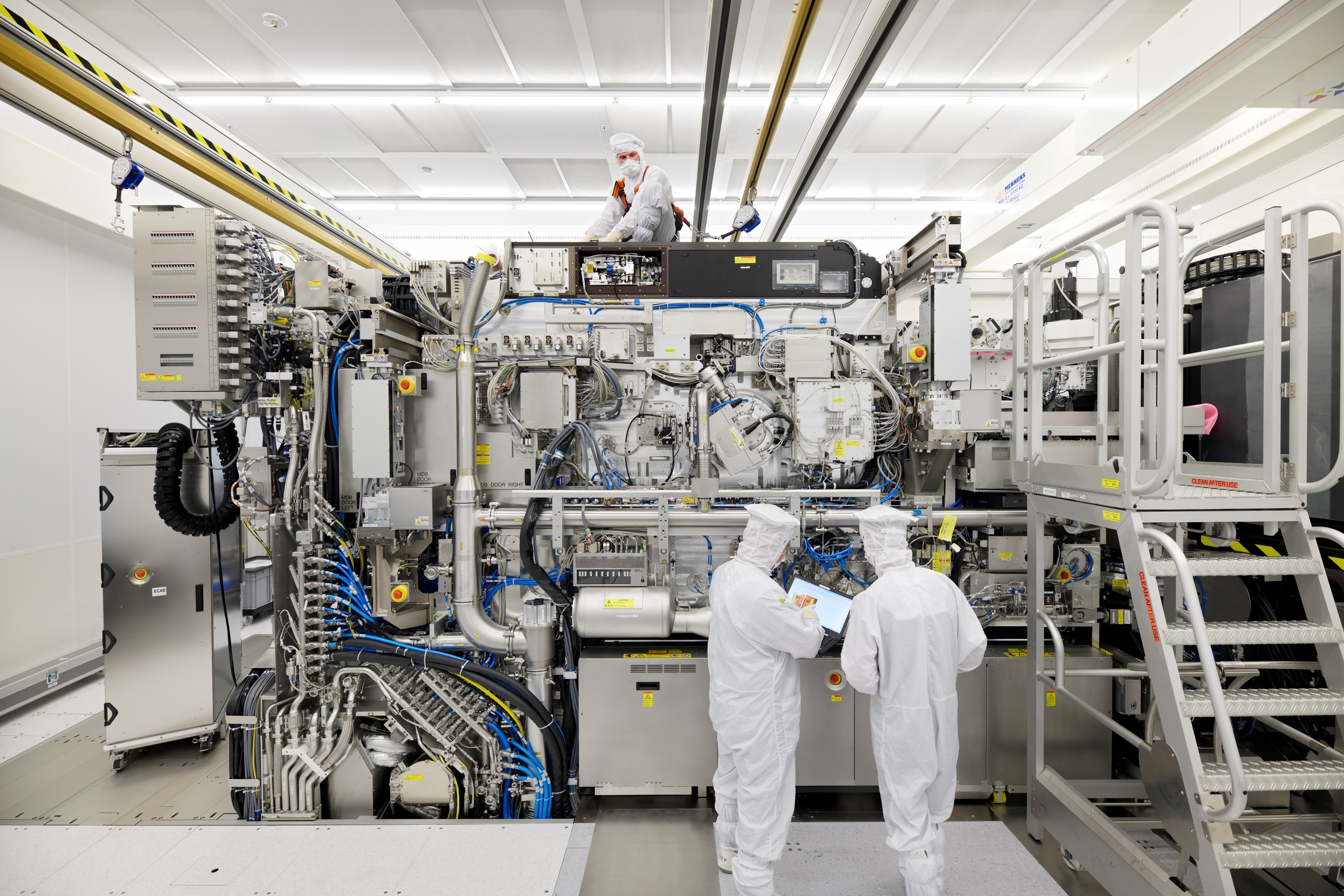
Employees are seen working on the final assembly of ASML’s TWINSCAN NXE:3400B semiconductor lithography tool with its panels removed, in Veldhoven, Netherlands. Image courtesy of Bart van Overbeeke Fotografie/ASML/Handout.
In some cases, a lithography machine for silicon wafer manufacturing may have a couple hundred thousand parts with dozens and dozens of kilometers of tubes containing wires feeding into them. That represents nearly countless opportunities for 3D printing to make an impact.
Of course, plastic prototyping is prolific across most high-tech industries, including semiconductor manufacturing. Metal 3D printing of end parts is beginning to grow in use. According to Green, there are already wafer processing systems on the market that include metal components made with 3D Systems equipment. This is in part due to the fact that the company has been serving the semiconductor equipment industry in Eindhoven, the Netherlands for the better part of a decade.
“We’re steadily increasing that pie chart of additive to non-additive parts in the leading-edge equipment with every generation—the latest products that are just being shipped. Now, in the generations beyond that, we’re seeing something like double or triple the number of additively manufactured parts inside of those than the machines that are in the market today,” Green said.
“Generally, what the silicon wafer manufacturers are trying to do is optimize the systems to reduce noise and uncertainty inside the systems so they can have faster time to market,” Green said.
To do this, a fast technology capable of rapid iteration is necessary. 3D Systems’ Direct Metal Printing (DMP), a form of laser powder bed fusion, is used by some firms to develop new machine designs.
Better thermal management of wafer tables can simultaneously improve semiconductor equipment accuracy by 1–2 nm, as well as speed and throughput. (Image courtesy of 3D Systems)
In some cases, end parts are produced that can lower tooling costs by combining multiple components in an assembly into a single part. These include wafer tables with complex cooling channels that might normally be made up of five to seven pieces machined and brazed together and have a two-to-three-month lead time. With AM, the same assembly can be made as a single piece more efficiently and with improved performance. Moreover, a variety of materials, such as copper or aluminum or titanium, might be tested to obtain the best thermal values.
“This is allowing the manufacturers to actually design for the function first, instead of making manufacturing compromises first, and then sacrificing function because of these compromises,” Green said.
The use of 3D printing in these businesses usually begins when either a manufacturer sees existing use cases from 3D Systems and reaches out to them or they experience their own technical issues and see an opportunity to overcome the challenge with AM. 3D Systems will then work with the customer on applications that are obvious and achievable, including wafer tables, manifolds, and general structural optimization.
3D Systems has two case studies that it has made public on its website, one of which is for what is probably considered the most complex piece of equipment on the planet: the Large Hadron Collider (LHC) at CERN. Representing the cutting edge of optics and physics, the LHC is looked at as the leading example for the semiconductor industry, with the technology developed for the massive particle physics experiment trickling down into semiconductor manufacturing.
The LHC example is discussed more fully in a separate article, but, in brief, Nikhef, the Dutch National Institute for Subatomic Physics, was aiming to produce leak-tight cool bars that could achieve -40˚C within the particle accelerator’s detector. Manufacturing the component with conventional processes was not feasible due to the required wall thinness, necessary to minimize the amount of material between the coolant and the surface to be cooled.
Working with 3D Systems, they were able to produce cool bars made from TiGr23. The leak-tight bars had wall thicknesses of just 0.25mm with 50-micron precision across the 263-mm length of the part. In turn, over 300 of these cooling bars were 3D printed using 3D Systems’ DMP technology.
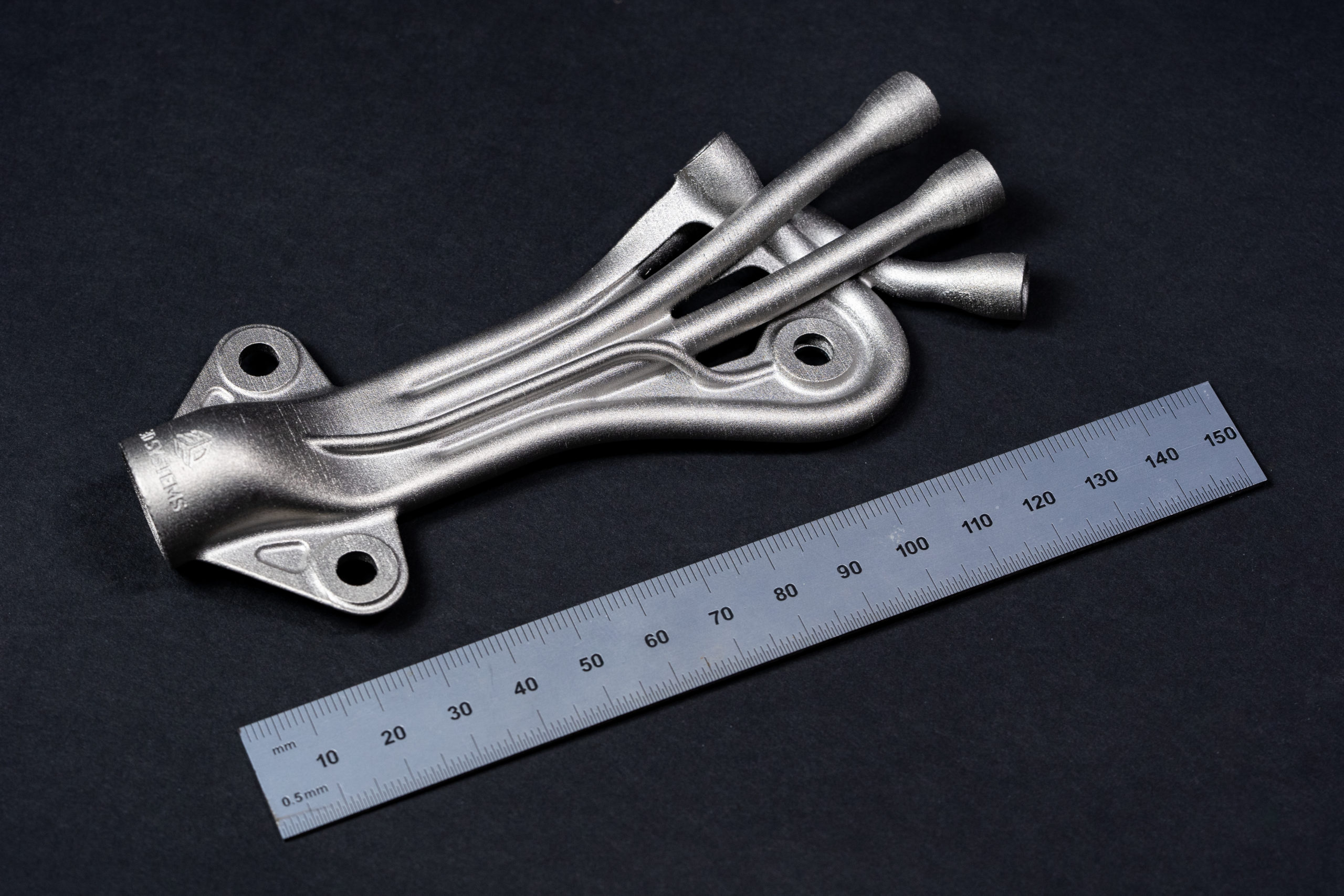
Cooling bars for the LHC. Image courtesy of 3D Systems.
The other case study is related to structural optimization to reduce vibration and improve the strength of wafer cooling tables and manifolds. Conventional manufacturing yields manifolds that are big, heavy, and create poor flow and connections. In contrast, Wilting , a tier 1 supplier for semiconductor OEMs, worked with 3D Systems to optimize fluid and gas flow within manifolds to reduce pressure drops, as well as mechanical disturbances and vibration.
When AM is employed to produce complex fluid manifolds, engineers can optimize designs to reduce pressure drop, mechanical disturbances, and vibration. (Image courtesy of 3D Systems)
Using additive manufacturing to create manifolds can help reduce liquid-caused disturbance forces by as much as 90 percent. Additionally, converting a multi-part assembly to a single 3D printed manifold has the potential to reduce weight by 50 percent. This, in turn, can lead to improved reliability, manufacturing and yield. The success of their partnership has driven increased demand for 3D printing with Wilting, which is expected to expand to Wilting’s customer base.
As a tier 1 supplier, Wilting is a good example of the direction adoption can go throughout the semiconductor manufacturing supply chain. Companies at that level are able to innovate freely with the OEMs for whom they work choosing to adopt those innovations when and where appropriate. If one of the five big manufacturers mentioned earlier (Intel, Samsung, etc.) sees the value of a new development, such as the use of 3D printing for metal end parts, it can push that development across its supply chain.
Lightweighting semiconductor components and advanced motion mechanisms reduces inertia and improves lithography and wafer processing machine speed and uptime. (Part courtesy of VDL)
This is being further driven by COVID and other supply chain trends, which are pushing OEMs to produce more innovative products more quickly. The CHIPS Act in the U.S., as well as legislation in the E.U., is seeing large rounds of funding directed at semiconductor production as businesses seek to reshore their operations and reduce dependence on China.
“There is a perfect storm creating an overwhelming amount of interest and speed around [AM in the semiconductor industry] because these companies are under a lot of pressure now. It’s just going to get ramped up with international funding and that Biden has pushed through,” Green said. “This means that, in the next two to five years, that shortage will be solved, but then you’ll have devices that’ll be on the market that will be a product of that funding. So smarter devices, lower costs, more memory, faster speeds, lower power usage—all the key values that you look for.”
With this in mind, increased adoption of AM in the semiconductor space is essentially inevitable. At the moment, part feature sizes and shapes aren’t too difficult, but Green sees 3D printing applied to ever-more difficult challenges, meaning components with very fine features and more complex geometries. Over the next 10 to 15 years, he sees the industry following a similar path to adoption of AM in aerospace, where the technology was first used outside of the engine compartment for brackets and aesthetic parts and is now increasingly used to completely reimagine engine designs.
“Especially as the part count of the latest machines increases, we’ll see more advanced thinking about AM in semiconductors. As they get past this optimization stage, where they’ve basically optimized as much as they can and are breaching the laws of physics, then they will start from scratch and think of some new ways to make wafers even better,” Green said. “That’s where things are going to get really interesting.”
In a decade or two, according to Green, design for AM will have been taught in undergraduate, graduate and trade schools so that engineers will be thinking about 3D printing from the outset when they enter the job market. This is in contrast to the current generation of experts who have to reorient their subtractive mindsets toward AM.
“Then, from a supply chain perspective, I see the opportunity for suppliers to transition to AM or fail and suffer. If your business is casting, assembly, and machining for the semiconductor industry, and that’s the lion’s share of your business, and you don’t shift to additive, you’re going to lose that business for sure,” Green concluded.
Subscribe to Our Email Newsletter
Stay up-to-date on all the latest news from the 3D printing industry and receive information and offers from third party vendors.
Print Services
Upload your 3D Models and get them printed quickly and efficiently.


You May Also Like
Bambu Lab A1 Used to Directly 3D Print Copper Electroplated Parts
Maker Dzingof was doing tonnes of electroplating of desktop and other 3D prints years ago with his Metalizzr project. I’ve been playing, a lot less successfully, with electroplated 3D prints...
3D Printing News Briefs, October 1, 2025: Bambu Lab Store, Shape-Morphing Materials, & More
In today’s 3D Printing News Briefs, Bambu Lab has opened its first retail store, and Meltio is inaugurating its first international additive manufacturing reference site. A consortium has launched a...
3D Printing News Briefs, August 13, 2025: Public Utility, Rocket Engine, Brains, & More
In today’s 3D Printing News Briefs, AML3D’s large-scale metal 3D printing system is now online at the largest public utility in the U.S. Moving on, Bright Laser Technologies is 3D...
Soft Robotics is Finally Coming Together: Northwestern Researchers Make Strides Towards a Better Actuator
Soft robotics for a long time was a lot of nice videos, papers, and very little in the way of useful technology. It was kind of an engineering Esperanto: a...