Researchers Model and 3D Print Graphene Electronic Devices


Made up of single atoms of carbon, graphene is thought to be a wonder material with a wide variety of applications, due to its high strength, lightweight, flexibility and unprecedented electrical conductivity. However, producing large graphene parts at scale remains a challenge. Previous research has shown that various methods for 3D printing graphene exist, but these techniques are still limited in size. Moreover, both these processes and non-additive methods for the production of large-area graphene layers hinder some of desired characteristics of the material, namely electrical conductivity.
Now, researchers at the University of Nottingham have developed a technique for 3D printing graphene using an inkjet technology that maintains the materials electrical properties, opening up possibilities for an array of electronic components, such as transistors and sensors. The study, titled “Inter-Flake Quantum Transport of Electrons and Holes in Inkjet-Printed Graphene Devices”, is published in the journal Advanced Functional Materials.
A 3D-printed phototransistor made up of “an exfoliated InSe flake contacted with six inkjet‐printed graphene stripes (each comprising 5 printed layers, 7 lines), which serve as electrodes, on a 300 nm SiO2/Si substrate.”
As a two-dimensional material, graphene is usually made by exfoliating individual layers of carob atoms in the form of a flat sheet. To then craft a multi-layer object of this material then requires hand-deposition of these sheets, an obviously laborious process. To fully exploit the properties of this wonder material through a scalable process, the University of Nottingham team developed a method for inkjetting inks loaded with flakes of graphene. Moreover, through the use of quantum mechanical modeling, the researchers are able to understand exactly how electrons move through the layers of graphene in order to control the electrical properties of the printed material.
Professor Mark Fromhold, Head of the School of Physics and Astronomy and a co-author on the paper, put it this way:
“By linking together fundamental concepts in quantum physics with state-of-the art-engineering, we have shown how complex devices for controlling electricity and light can be made by printing layers of material that are just a few atoms thick but centimeters across. According to the laws of quantum mechanics, in which the electrons act as waves rather than particles, we found electrons in 2D materials travel along complex trajectories between multiple flakes. It appears as if the electrons hop from one flake to another like a frog hopping between overlapping lily pads on the surface of a pond.”
To print the material, graphene inks made up of graphene flakes and ethyl cellulose, were dispersed into a mixture of cyclohexanone/terpineol and printed onto a substrate using a drop-on-demand method. The layers were then annealed in a vacuum oven at 250°C to remove the solvent and breakdown the additives within the ink. The team found that the greater the number of layers, the lower the electrical resistance. To demonstrate the possibilities of the material, the team 3D printed a phototransistor made up of graphene electrodes printed onto a semiconducting crystal.
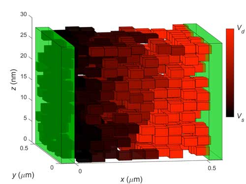
A simulation of packed graphene flakes between two contacts.
Key to the research was understanding the movement of electrons in order to best produce graphene parts. To do this, the team modeled the conductive properties of the network of flakes within the printed parts, simulating the charge transfer between flakes of graphene as virtual voltage is applied to a simulated device. The authors note: “Our model reveals the mechanism of carrier transport in printed graphene layers and shows that optimized thickness of printed layers with high [packing fraction] is required to achieve high conductivity devices.”
To understand how printed graphene would work within a device made of multiple types of materials, the researchers 3D printed a field-effect transistor. The electrical resistance was actually higher than expected for five printed layers of graphene due to the mixing of inks between layers.
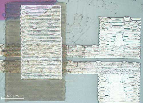
Optical microscopy image of the 3D printed graphene field-effect transistor; “scale bar is 500 µm, spacing between silver electrodes is 100 µm.”
Co-author, Dr Lyudmila Turyanska from the Centre for Additive Manufacturing, said of the work:
“While 2D layers and devices have been 3D printed before, this is the first time anyone has identified how electrons move through them and demonstrated potential uses for the combined, printed layers. Our results could lead to diverse applications for inkjet-printed graphene-polymer composites and a range of other 2D materials. The findings could be employed to make a new generation of functional optoelectronic devices; for example, large and efficient solar cells; wearable, flexible electronics that are powered by sunlight or the motion of the wearer; perhaps even printed computers.”
Next, the team plans to refine the deposition of the graphene through the use of polymers in order to impact the way that flakes align. They also hope to use different types of inks with varying sizes of graphene flakes. The researchers will also improve their computer simulations to include how the different materials work together. Finally, they aim to develop methods for mass production of the prototyped devices.
Subscribe to Our Email Newsletter
Stay up-to-date on all the latest news from the 3D printing industry and receive information and offers from third party vendors.
Print Services
Upload your 3D Models and get them printed quickly and efficiently.


You May Also Like
GKN Aerospace & Pratt & Whitney to Use Additive for the F135 Engine
GKN Aerospace and RTX unit Pratt & Whitney will collaborate on additive manufacturing for the F135 engine. This is an important engine. The turbofan powers the F-35 Lightning II, but...
Zaha Hadid Architects Print 6M Model with WASP’s Robotic Arm Solutions
Zaha Hadid Architects (ZHA) have successfully used WASP 3D printers to make a 6-meter-tall model of an aircraft control tower. Zaha Hadid Architects’ Tech Lab made the tower in-house for the ZHAviation...
3DPOD 303: 6K Additive CEO Frank Roberts on Premium and Sustainable Metal AM Powder
6K Additive is roaring ahead with a recycling solution for metals. Their path from scrap to powder is helping the US to be more resilient, produce powder locally and perhaps...
3D Printing News Briefs, June 18, 2026: Reseller, Relocation, Metal Space Powder, & More
We’ll start with business news in today’s 3D Printing News Briefs, as XJet appointed a value-added reseller in Germany, BIO INX is expanding its presence in the Italian market, and...