

These things can change at any moment nowadays, but the biggest economic story of the year might not be elevated energy prices, after all. Elevated prices for memory chips may end up being the most lasting trend to emerge in 2026.
Share prices for chipmakers like Micron surged throughout H1 thanks to skyrocketing demand for memory and storage chips, a trajectory that led Apple to announce it would be raising prices on certain products. This is the immediate backdrop for another trend I’ve been writing about all year, the change in the semiconductor capital equipment (semicap) market that I’ve framed as an “insurrection”. The ability to design semiconductor devices in 2.5D/3D has led to innovations surrounding chipmakers’ fanned out and/or stacked packaging of memory dies and compute dies, creating an alternative (“System-in-a-Package”) to what had become the market standard (“System-on-a-Chip”).
Chipmakers have experimented with a variety of methods, including additive manufacturing (AM), to execute their designs, and companies such as Poland’s XTPL have been the beneficiary. XTPL is an original equipment manufacturer (OEM) of a printhead, the Ultra Precise Dispensing (UPD) module, as well as various printers leveraging the UPD, like the Delta Printing System (DPS). It has a portfolio of customers spanning from mainland China and Taiwan to Silicon Valley and, most recently, to Japan.
After first announcing its entry into the Japanese market just last month, XTPL is already announcing that it has made a sale to a new customer in Japan, following work by XTPL and the unnamed Japanese company to validate the DPS process for electronics packaging. Notably, XTPL will also sell the customer “a dedicated laser system” that will enable printing of copper conductive paths.
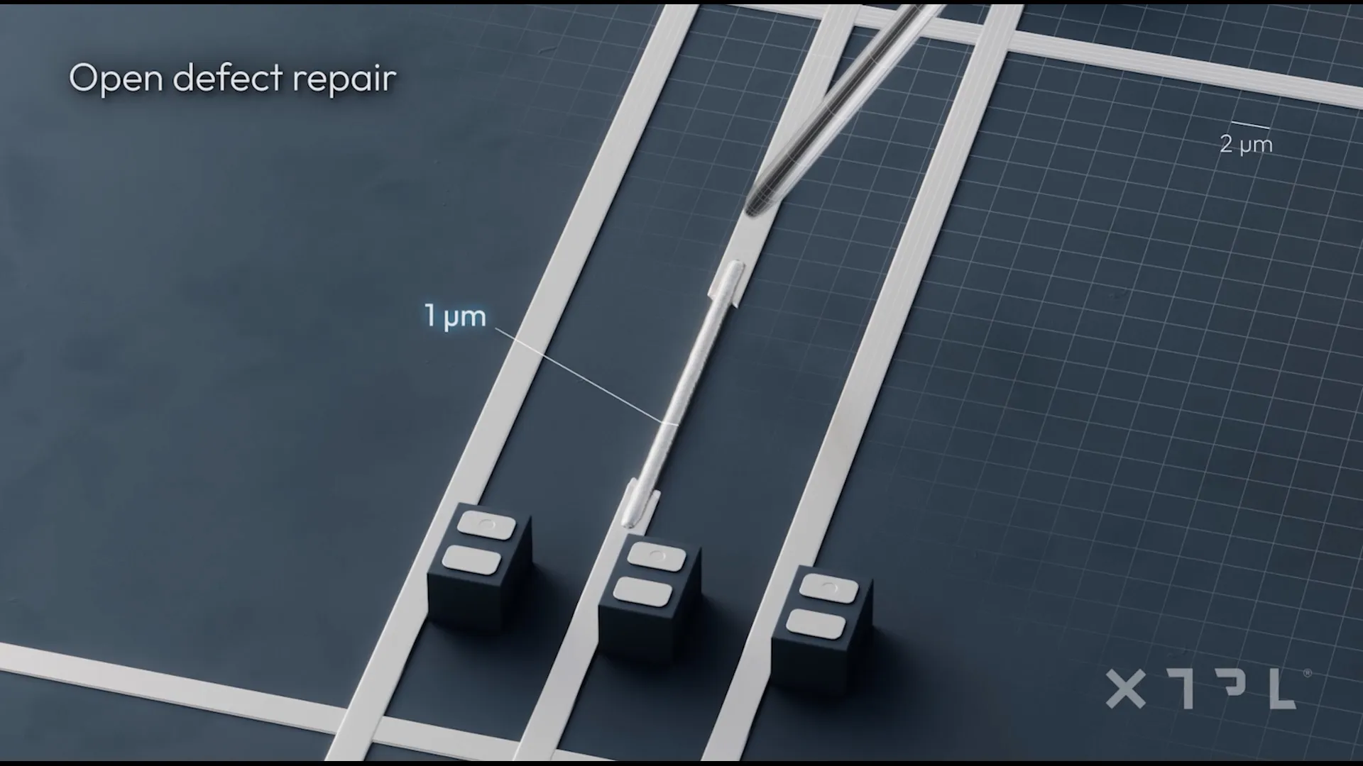
That’s similar to the work XTPL did as part of the previously announced sale into the Japanese market, implying growing demand from semicap OEMs for AM packaging capabilities. As I mentioned in my previous post on XTPL, the company’s business strategy is built around guiding customers through a clearly defined pathway from R&D to serial production, giving each initial sale (like the one at the focus of the present post) heightened potential to transform into repeat business of higher value hardware.
In a press release about XTPL’s sale to a new Japanese customer shortly after its first-ever sale in Japan, XTPL’s CEO, Filip Granek, said, “We are pleased to announce another sale in the demanding Japanese market, particularly as this order comes from a new client and relates to a project entirely separate from the sale of the UPD module reported in June. In this case, the client has decided to purchase a DPS device, which will enable it to independently validate XTPL’s technology in its own R&D laboratory.
“In our terminology, this marks the progression of a project with industrial deployment potential to the third stage of this process, following the successful completion of validation tests carried out jointly by the client and our laboratory in Wrocław. We therefore see a very important sign of the replicability of our commercial model: a second independent partner in Japan is advancing a project in the same strategic application area – yield management for HDI/UHD PCBs and semiconductor substrates used in advanced packaging for semiconductor technologies – using our copper nanoink. Japan remains one of the world’s most technologically advanced industrial markets, which is why another client engagement in this country is of particular importance for strengthening XTPL’s global brand.”
Now, an especially interesting angle to the context described in the first couple of paragraphs is that shares for memory chipmakers have plummeted following their epic run in the first half of the year, echoing the sell-off in energy stocks (and futures) after a historically bullish Q1 for energy investors. This isn’t so surprising: while investors’ brains are conditioned to view chips as “tech,” memory chips are in fact cyclical commodities that tend to follow notoriously volatile boom-bust cycles.
The interesting part, however, is that the genuine revolution going on in advanced chip packaging could in the long run help companies like Micron, SK Hynix, etc., avoid the turbulence of past memory boom phases. If chiplet design can enable relatively on-demand production of more customized chip architectures for major semiconductor customers, it could help semiconductor OEMs avoid growing production capacity beyond the market’s appetite.
In fact, we’re already seeing companies like Google, Meta, and the like pivot towards developing their own custom AI chip architectures. The key is in ensuring that broadly accessible packaging solutions mature to meet customers where they’re at. XTPL’s activity throughout 2026 appears to be evidence that this is the strategy semicap OEMs are deploying.
It’s certainly likely that the long-term floor for memory chips has permanently risen, but wider adoption of AM for advanced packaging could potentially keep the long-term price ceiling within reasonable limits, which would help suppliers avoid the demand destruction caused by scarcity-induced price spikes.
Images courtesy of XTPL