
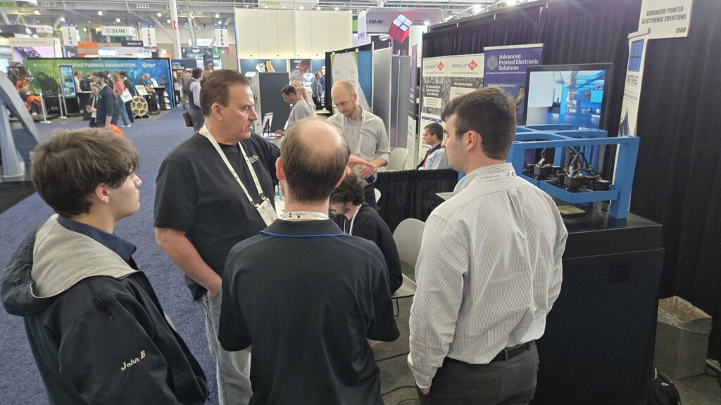
I didn’t attend RAPID + TCT this year, so I missed getting to see the Matrix6D platform operating live on the show floor. Thankfully, the CEO and founder of Advanced Printed Electronics Solutions (APES), Dr. Rich Neill, sent a video of the demonstration to 3DPrint.com, which you can watch below:

If you’re unfamiliar with APES and Matrix6D, Joris Peels’ 2025 article on the platform, written following its first public unveiling at last year’s RAPID + TCT, provides a highly useful summary. You can also read the article I wrote on APES earlier this year about the partnership that the company formed with Great Lakes Semiconductor.
Many paradigm shifts are occurring simultaneously in the global economy right now, and one involves the semiconductor sector. And, because of how singularly consequential the semiconductor sector is to the global economy, it’s very possible that all of the other shifts are being triggered (if only indirectly) by the semiconductor paradigm shift. However, we don’t need to get into that right now. The point is that electronics manufacturing is on the brink of a transformation as pivotal as the invention of semiconductor photolithography in the 1950s, and APES is the sort of company embodying that change.

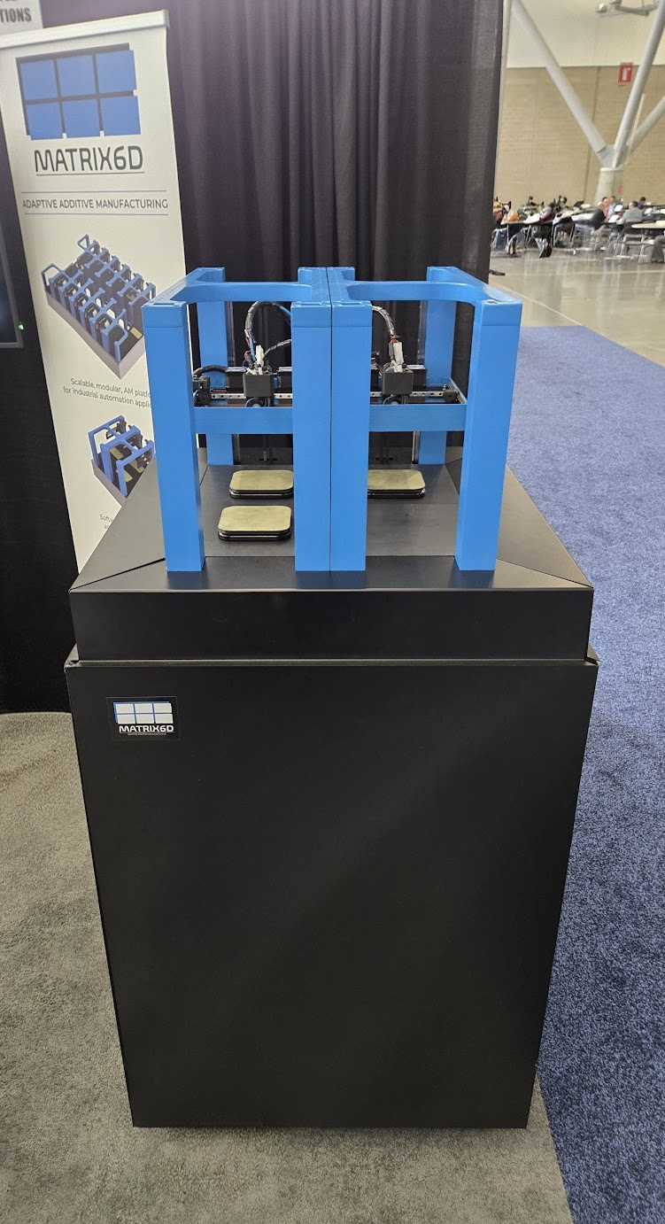
The Matrix6D platform on the show floor at RAPID + TCT 2026. Image courtesy of APES.
The transformation involves many distinct elements, but the primary ones are probably innovations in both chip design and semiconductor capital equipment (semicap). In a recent article, part of my “AM Demand Signals” series, I called this “the Semicap Insurrection,” which I think starts to hint at the stakes involved. Here’s how I explained the chip design component in that earlier article:
“…chip design that moved beyond 2D to 2.5, and 3D was “the silent economic revolution of the 2010s.” Shifting the design of integrated circuits (ICs) from logic that only worked in a side-by-side arrangement to a logic that fully incorporates the z-axis has enabled a complete reimagining of how semiconductor devices can be created. In addition to the System-on-a-Chip (SoP) model, semiconductor OEMs are now also starting to see how far they can go with chiplets: the System-in-a-Package (SiP) model defined by stacking a number of less sophisticated dies. Increasingly, AM is the tool that the new wave of semicap OEMs are leveraging to deliver the advanced package necessary to produce chiplets.”
I followed up on that article with a PRO article on Elon Musk’s official announcement of Terafab, in which I argued that the world’s richest man is likely aiming to leverage the likes of TSMC into helping him build a chiplet packaging ecosystem on US soil. As it turns out, TSMC and other global chip giants have their own name for the Semicap Insurrection, which is “Foundry 2.0.” One of the core principles of this evolution in the foundry business model is a move beyond focusing solely on wafer fabrication, towards encompassing all aspects of the process — most notably, advanced packaging — and diversifying beyond exclusive reliance on fixed capital at a handful of sites to systems integration services on a customer-by-customer basis.
Albeit on a much smaller scale, this is essentially the sort of deal that APES made with Great Lakes Semiconductor, with the latter planning to use the Matrix6D as a linchpin of its Fab-as-a-Service (FaaS) model. A key to understanding why the semiconductor sector is making this change is the economic necessity of delivering high-mix, low-volume batches produced on-demand. Anyone familiar with the most compelling selling points of AM more broadly can instantly grasp why the technology is indispensable to enabling that pivot.
Now, beyond the reasons why the semiconductor industry is moving in the direction I’ve laid out, it’s worth considering what we might expect as the implied changes become more commonplace. The APES video from RAPID is a perfect reference point for gaming out the possibilities. The chipmaking process has always happened in isolation from the rest of society, with very little transparency into the inner workings of a fab.
Suddenly, chipmaking is something that can be demonstrated on a trade show floor, creating the preconditions for bringing more minds than ever before into the semiconductor design process. Historically, the semiconductor industry has more or less reinvented itself once or twice a generation. There have never been more opportune circumstances for the next wave of reinvention to happen.
Thomas Kuhn, the philosopher who originally coined the term “paradigm shift” in his book The Structure of Scientific Revolutions, wrote, “What man sees depends both upon what he looks at and also upon what his previous visual-conception experience has taught him to see.” Paradigm shifts happen when enough people look at the world as it is and recognize that things are starting to emerge that change the very definition of what’s possible.
That’s the type of vision required to create something like the Matrix6D. Now that it exists right before the eyes of the general public, the real fun starts: who knows what possibilities it will open up?