
It’s been just a few weeks since NASA announced their plans to invest in a new type of 3D printing technology dubbed Selective Separation Sintering (SSS), which was developed by the NASA In-Situ Materials Challenge winner, Dr. Behrokh Khoshnevis. A couple of days ago, the space agency also revealed that they have their sight set on innovating upon other styles of 3D printing techniques as well. One team of technologists from NASA’s Goddard Space Flight Center, which is located in Greenbelt, Maryland, have been looking into a 3D printing process called aerosol jet printing (aka direct-write manufacturing). This technology, which has been recently pioneered by the Albuquerque, New Mexico-based company Optomec, is well-suited for fabricating high performance electronic components, and could potentially help NASA researchers construct more densely populated electronics.

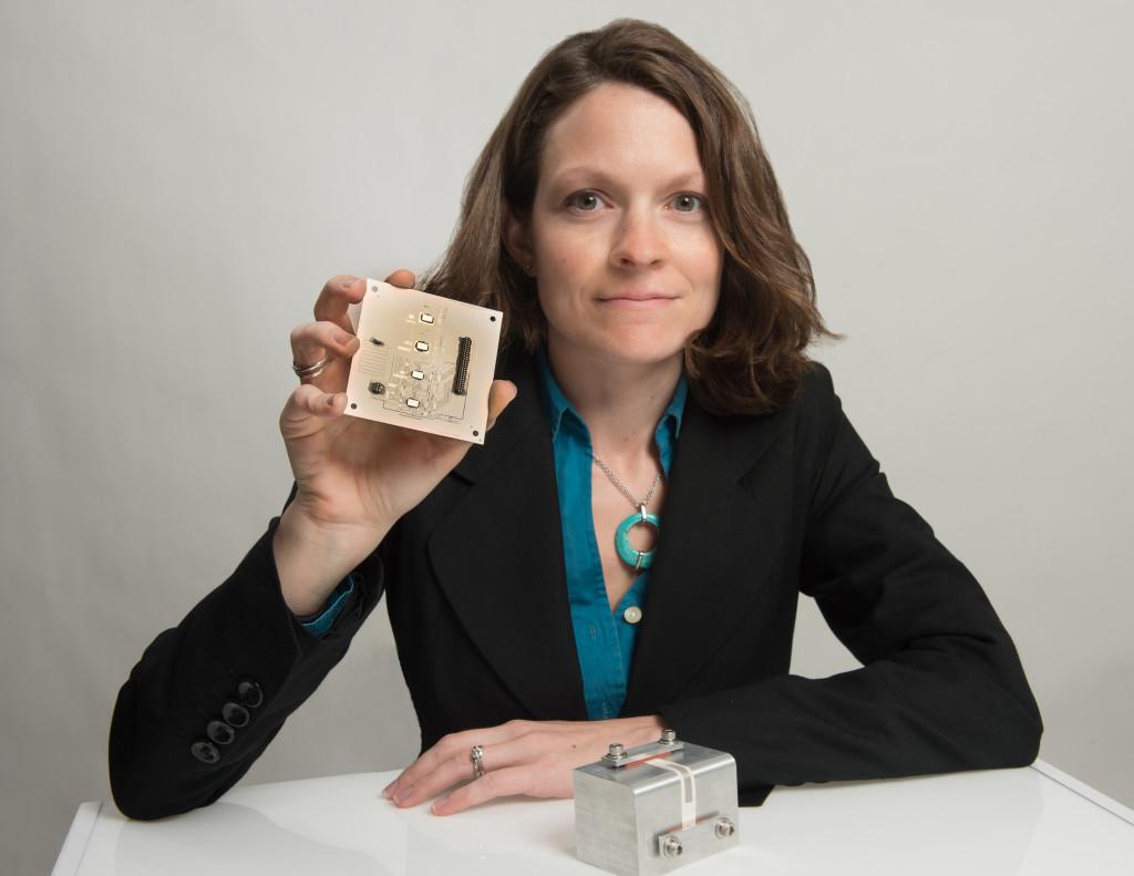
Beth Paquette holds the 3 x 3 inch ceramic board, which was populated with four radiation-hardened digital-to-analog converter chips and connected with a 3D printed silver ink.
The aerosol jetting technique is a bit different than your everyday FDM printer. Although it does build components layer by layer, the process works by using a carrier gas and printer head, which together deposits a fine aerosol of metal particles onto the surface bed. Aerosol jet printing is compatible with a handful of metal materials, including silver, gold, platinum, and aluminum, and can even deposit polymers and other insulators as well. This unique 3D printing technology could serve as an ideal solution for many applications both in space and on Earth, particularly for manufacturing NASA’s detector assemblies, which have become both smaller in size and more densely populated with electronic components over time.

“If we succeed, aerosol jet technology could define a whole new way to create dense electronic board assemblies and potentially improve the performance and consistency of electronic assemblies,” explained Goddard Space Flight Center technologist Beth Paquette. “Furthermore, aerosol jet printing promises to slash the time it takes to manufacture circuit boards, from a month to a day or two.”
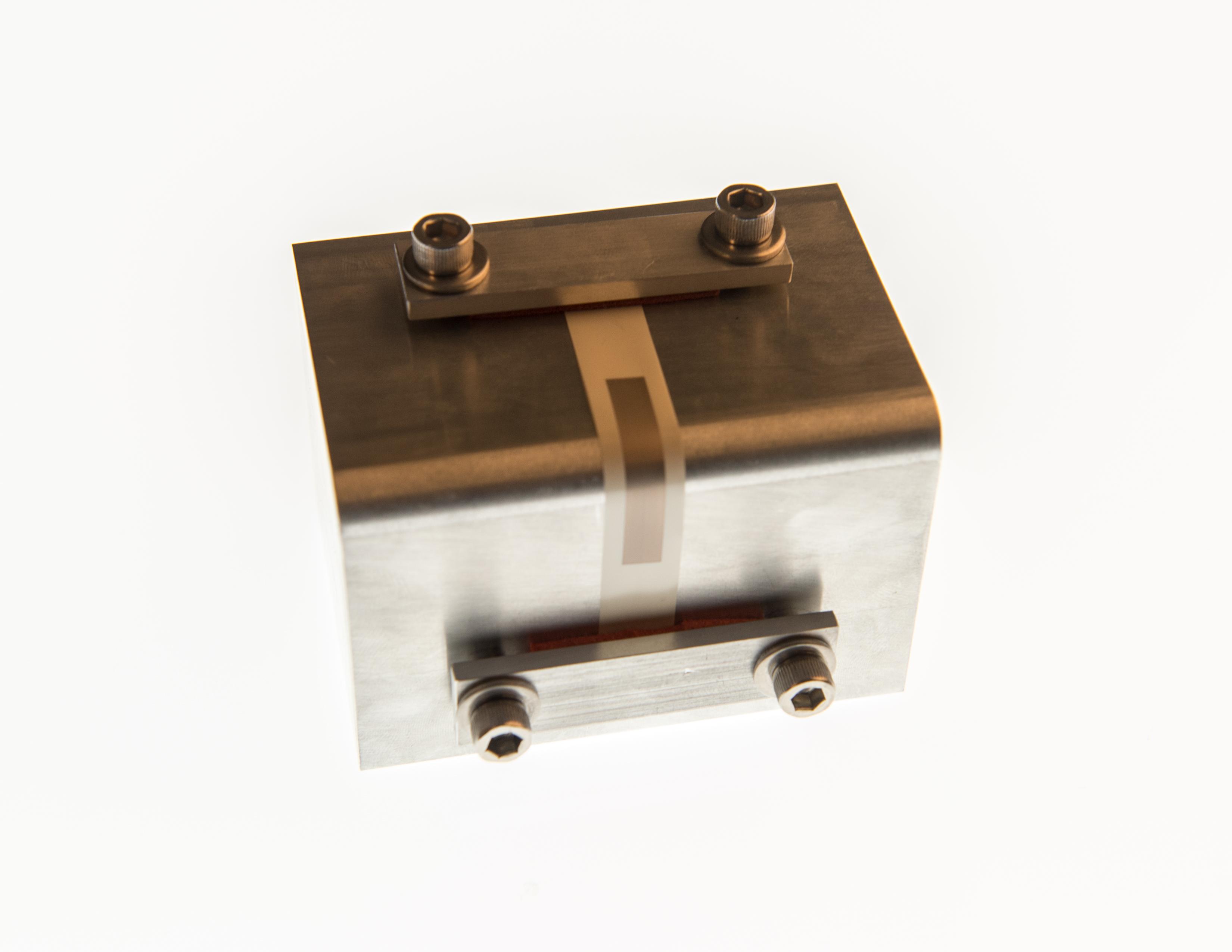
Liquid crystal polymer (LCP) strip containing gold traces or wires that were printed with aerosol jet printing
Though a big focus of the study seems to be on manufacturing detector assemblies, there are a number of other NASA-related applications that aerosol jetting could be highly beneficial for. The 3D printing technology could also be used by NASA in the near future to print antennas, wiring harnesses, and other types of hardware directly onto a spacecraft. Thus far, Paquette and her team have already produced a 3 x 3 inch ceramic board, which was populated with four radiation-hardened digital-to-analog converter chips and connected with a 3D printed silver ink. Though Goddard team acknowledges the potential uses of aerosol jetting technology, they’ve yet to test printed components under typical flight conditions. With spaceflight application in mind, the researchers are currently observing the repeatability and robustness of this unique printing process.
The project involves aerosol jetting technology company Optomec, along with other industry groups such as NanoDirect LLC, Raytheon, and United Technologies Research Center. In addition, the study also enlisted the assistance of NASA’s Marshall Space Flight Center, the National Institute of Standards and Technology, the University of Maryland’s Laboratory for Physical Sciences, the University of Delaware, Georgia Tech, and the University of Massachusetts-Lowell. For their next move, the Goddard Space Flight Center research team is likely to test these aerosol jetted electronics under actual spacecraft flight conditions. Discuss in the Using Aerosol Jetting to 3D Print Detector Assemblies forum over at 3DPB.com.
[Source: NASA / Images: NASA/W. Hrybyk]