![]()
In just the last year or two we’ve seen unprecedented advancements in the areas of medical and dental 3D printing, in metal 3D printing and the ability to rapidly produce working end-use quality prototypes. And of course, the development of technology that allows for seamless 3D printing with multiple materials so we can have those 3D printed electronics.
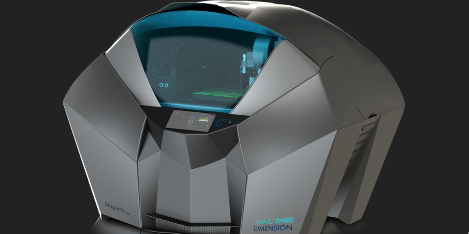
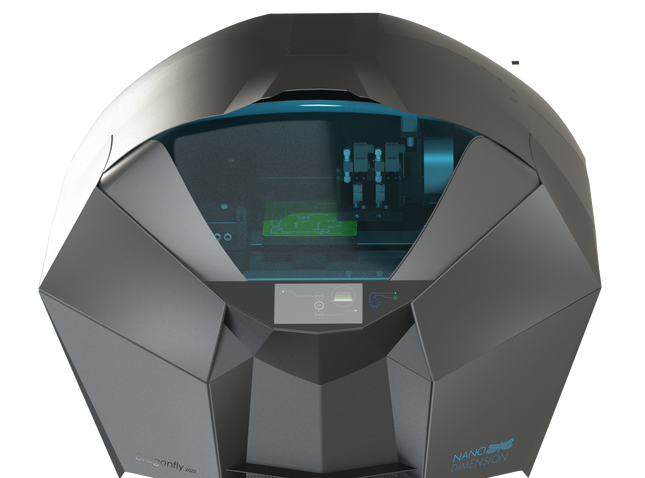
The 3d printing Industry may have just gotten one step closer to finding its Holy Grail with the announcement of Nano Dimension’s new PCB – Printed Circuit Board – 3D printer. The Dragonfly 2020 3D Printer is a 3D inkjet deposition printer that can print complete, multi-layer circuit boards using insulating and conductive nano-inks.
“The Nano Dimension PCB printer is a highly accurate and versatile inkjet deposition system for printing multi-layer circuit boards. The innovative hardware, dedicated nano-inks and novel software bring new possibilities to a wide range of R&D, prototyping and custom manufacturing projects. Our highly conductive silver nano-inks are also available separately,” explained Nano Dimension on their website.
Take a look at this Nano Dimension promotional video explaining the technology and it’s potential uses:
In house production of PCBs will enhance a typical product designer’s ability to experiment with their projects quickly, and cut down development and eventually consumer costs. Not only will this allow designers a greater amount of freedom in the prototyping phase of consumer electronics production, but it allows companies to maintain tight control over their intellectual property during the development phase.
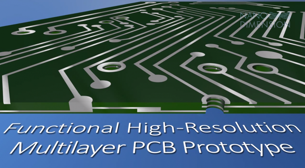
As with most deposition 3D printers, the complexity of the design is virtually irrelevant due to the lack of required support material. The circuit boards that are capable of being printed can be ten or more layers of interconnected, ready to use, ready to be soldered circuits. This makes the Dragonfly 2020 ideal for advanced prototyping and even small batch manufacturing. Currently the printing envelop is 20cm x 20cm, however once production of the first model has begun Nano Dimension does have plans to develop printers with larger printing envelopes.
The process is also an excellent green option, as many of the chemicals and waste materials associated with PCB production are virtually eliminated, and the nano-inks are not considered hazardous waste. There is very little post processing involved as the Dragonfly 2020 has an integrated sintering process that will cure the ink until it reaches the desired conductivity and surface adhesion.
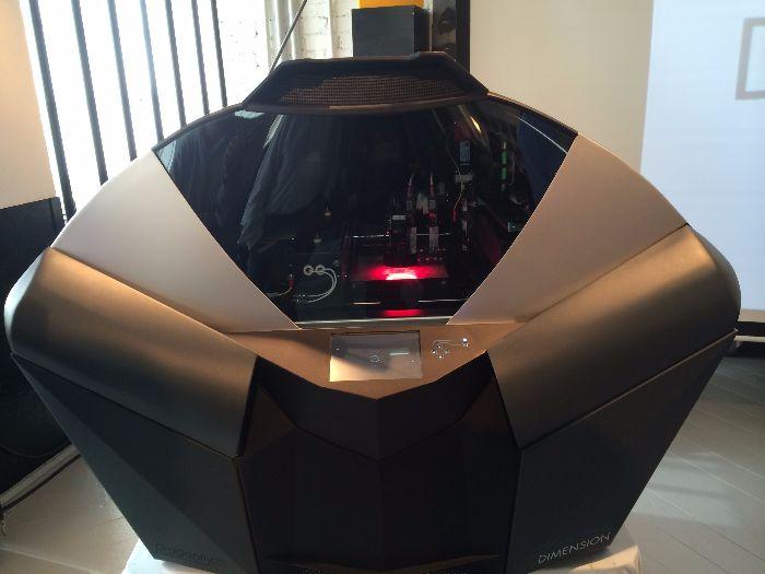
The printer was announced by 3D printing firm Nano Dimension at a special presentation on April 14th in Tel-Aviv. The Israeli company presented its first working prototype and unveiled their plans to have the production model available for purchase in mid to late 2016. At this time there has not been a price point given, however it is not expected to be friendly to the home market. How would you use a PCB 3D printer? Tell us about it over in the Dragonfly 2020 Multi-Layer Circuit Board 3D Printer forum at 3DPB.com.