Now a new 3D imaging chip, developed by researchers at the California Institute of Technology, has been made small enough to fit inside a smartphone and will soon be ready to let consumers take a 3D image of an object with their phone, for later replication with a 3D printer. The data used to construct 3D prints requires the creation of a digital model with height, width and depth information, and until now, a 3D scan of an object was required to create that model.


Professor Ali Hajimiri
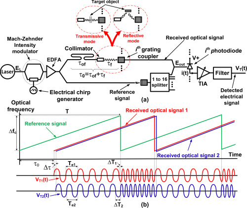
According to Ali Hajimiri, the Thomas G. Myers Professor of Electrical Engineering in the Division of Engineering and Applied Science at Caltech, the technology is based on an inexpensive, tiny and highly accurate device known as a nanophotonic coherent imager, or NCI.
Making use of an inexpensive silicon chip less than a square millimeter across, theses NCIs provide superb depth measurement accuracy, and the silicon photonics are an ideal platform for coherent 3D imaging and projection systems with high resolution and pixel counts.
“Each pixel on the chip is an independent interferometer – an instrument that uses the interference of light waves to make precise measurements – which detects the phase and frequency of the signal in addition to the intensity,” says Hajimiri of the chips.
The new chip uses LIDAR technology which targets an object illuminated with scanning laser beams. As light that reflects off of the object, it’s analyzed based on the wavelength of the laser light used and the LIDAR system is used to gather information about the size and its distance from the laser of an object to create an image of its surroundings.
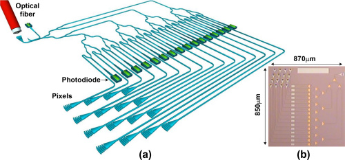
“By having an array of tiny LIDARs on our coherent imager, we can simultaneously image different parts of an object or a scene without the need for any mechanical movements within the imager,” Hajimiri says. “By coupling, confining, and processing the reflected light in small pipes on a silicon chip, we were able to scale each LIDAR element down to just a couple of hundred microns in size – small enough that we can form an array of 16 of these coherent detectors on an active area of 300 microns by 300 microns.”
The IR wavelengths can be processed efficiently by integrated silicon-on-insulator (SOI) nanophotonic platforms, and the researchers say they have the potential to ultimately be integrated with silicon electronics to create NCIs with a large number of pixels in a small area – and at a very low cost.
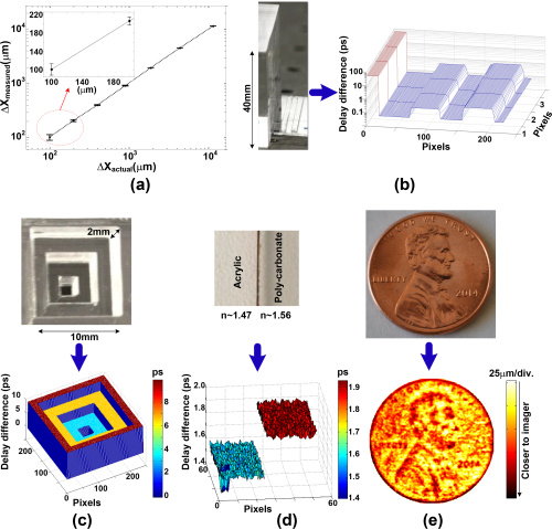
Hajimiri and his colleagues have used the device to scan and build a 3D image of the “hills and valleys” impressed on the face of a penny down to micron-level resolution from just half a meter away.
Hajimiri says the current array of 16 pixels will soon be scaled up to hundreds of thousands of pixels and result in vast arrays of LIDARs.
“The small size and high quality of this new chip-based imager will result in significant cost reductions, which will enable thousands new of uses for such systems by incorporating them into personal devices such as smartphones,” he says.
The study, entitled “Nanophotonic Coherent Imager,” was authored by Hajimiri, Firooz Aflatouni, Behrooz Abiri and Angad Rekhi, and it was published in the February issue of Optics Express.
Can you imagine any applications for these tiny, LIDAR-driven chips? Let us know in the Tiny Chip From Caltech forum thread on 3DPB.com.