

Arik Gordon
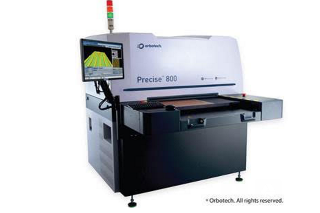
This new system was in good company for launching at CTEX, with a wide range of PCB technology and materials being exhibited. The Precise 800 is unique as the first solution for advanced high density interconnect (HDI) and complex multi-layer PCB manufacturing. The new technology should attract the attention of PCB manufacturers as it’s capable of removing excess copper as well as filling in the areas where it is missing. These features are significant as it means the ‘shaping solution’ is eliminating scrap and offering substantial savings on the bottom line with a rapid recoup regarding the initial investment.
“The Precise 800 is a unique innovative implementation of digital additive manufacturing and represents a complete breakthrough in electronics micro-manufacturing production processes,” said Arik Gordon, Corporate Vice President and President of Orbotech’s PCB Division. “It is based on an additive technology that was developed by Orbotech over a number of years.”
Two proprietary Orbotech technologies are at work:
3D Shaping (3DS) technology is based on a series of processes that includes 3D defect analysis, 3D laser shaping and 3D visualization. By comparing the shape of the defect with real-time computer-aided manufacturing (CAM) data and simultaneously conducting 3D analysis, 3DS automatically identifies where copper needs to be added. It then guides the system’s laser to Orbotech’s Precise Stick, a high-quality metal carrier, for precise copper deposition. The results can be confirmed immediately with 3D visualization.
Closed Loop (CLS) technology employs specialized image analysis algorithms to make real-time comparisons between the actual image and the design data (CAM) to find the precise location of the shorts and opens. It then intelligently guides the system’s laser to ablate excess copper with high accuracy.
“Our customers are under continual pressure to produce cost-sensitive, ever-smaller, functionality-rich devices in high volumes,” said Gordon. “The Precise 800 meets their requirements by providing high-quality, meticulous shaping of PCBs that might otherwise have been scrapped.”
This system is available for sale now to customers globally, and if you are interested in purchasing one or finding out more, contact Orbotech.
Orbotech is a global provider of solutions for electronics reading, writing, and connecting used by manufacturers of printed circuit boards, flat panel displays, advanced packaging, micro-electro-mechanical systems, and other electronic components. Virtually every electronic device in the world is produced using an Orbotech system. Discuss further in the Orbotech 3D Shaping Technology forum over at 3DPB.com.